TEM vs SEM: Choosing the Right Electron Microscopy for Nanoparticle Characterization in Drug Development
This article provides a comprehensive, comparative guide for researchers and pharmaceutical scientists on using Transmission Electron Microscopy (TEM) and Scanning Electron Microscopy (SEM) for nanoparticle size and shape analysis.
TEM vs SEM: Choosing the Right Electron Microscopy for Nanoparticle Characterization in Drug Development
Abstract
This article provides a comprehensive, comparative guide for researchers and pharmaceutical scientists on using Transmission Electron Microscopy (TEM) and Scanning Electron Microscopy (SEM) for nanoparticle size and shape analysis. We cover foundational principles, detailed methodological workflows, common troubleshooting for sample preparation and imaging artifacts, and a direct validation-based comparison of resolution, quantification accuracy, and suitability for different nanomaterial classes (e.g., lipid nanoparticles, polymeric micelles, inorganic carriers). The goal is to empower professionals to select and optimize the right technique to meet rigorous regulatory and research standards in nanomedicine development.
Nanoparticle Imaging Fundamentals: Core Principles of TEM and SEM Explained
Nanoparticle-based therapeutics and diagnostics represent a paradigm shift in medicine. However, their efficacy, biodistribution, and safety are intrinsically linked to physicochemical properties, with size and shape being paramount Critical Quality Attributes (CQAs). Electron microscopy (EM), specifically Transmission (TEM) and Scanning (SEM) Electron Microscopy, provides the necessary nanoscale resolution to characterize these CQAs directly, making it an indispensable tool in nanomedicine research and quality control.
The Analytical Framework: TEM vs. SEM for Nanoparticle CQA Analysis
The choice between TEM and SEM is dictated by the specific information required. A comparative analysis, based on a synthesis of recent literature and practical applications, is summarized below.
Table 1: Comparative Analysis of TEM and SEM for Nanoparticle Size and Shape Characterization
| Feature | Transmission Electron Microscopy (TEM) | Scanning Electron Microscopy (SEM) |
|---|---|---|
| Primary Interaction | Electrons transmitted through the specimen. | Electrons scattered from the specimen surface. |
| Resolution | ≤ 0.1 nm (theoretical), ~0.5 nm (practical for nanoparticles). | 0.5 nm to 1 nm (for high-end field-emission guns). |
| Image Type | 2D projection of internal structure. Provides crystallographic data via diffraction. | 3D-like topographical image of surface. |
| Size Measurement | Direct measurement of primary particle diameter (core). Accurate for size distribution. | Measurement includes surface coatings/hydration shell. Excellent for agglomerate size. |
| Shape Analysis | Excellent for definitive shape (spheres, rods, cubes, triangles) and core morphology. | Excellent for 3D topography and overall particle shape. |
| Sample Preparation | Complex: requires thin support films (<100 nm), often involves staining. | Simpler: requires conductive coating for non-conductive samples. |
| Throughput | Lower; detailed imaging and analysis per particle. | Higher; can survey large sample areas quickly. |
| Key Application in Nanomedicine | Definitive core size/shape, crystallinity, shell thickness (for core-shell), degradation. | Surface morphology, aggregation state, interaction with substrates/cells. |
Detailed Experimental Protocols
Protocol 1: TEM Sample Preparation and Imaging for Liposomal Drug Formulations
Objective: To determine the core size distribution, lamellarity, and morphological integrity of PEGylated liposomes.
Materials:
- Purified liposomal suspension.
- 200-400 mesh Copper grids with continuous carbon or ultrathin carbon on holey support film.
- Glow discharge unit.
- 2% (w/v) Uranyl acetate solution or 1% Phosphotungstic acid (PTA), pH 7.0.
- Filter paper (Whatman No. 1).
- Precision pipettes.
- High-Resolution Transmission Electron Microscope (e.g., JEOL JEM-1400Plus, Thermo Fisher Talos).
Procedure:
- Grid Activation: Subject the carbon-coated grids to a low-pressure argon plasma glow discharge for 30-45 seconds to create a hydrophilic surface.
- Sample Application: Pipette 5-10 µL of the diluted liposome suspension onto the grid surface. Allow to adsorb for 1 minute.
- Negative Staining: Wick away excess liquid with filter paper. Immediately apply 10 µL of uranyl acetate stain for 30 seconds.
- Washing: Wick away the stain and gently touch the grid to a drop of deionized water (3 times) to remove excess stain.
- Drying: Allow the grid to air-dry completely in a clean, dust-free environment.
- Imaging: Insert the grid into the TEM holder. Image at an accelerating voltage of 80-100 kV to minimize beam damage. Use low-dose techniques. Capture micrographs from multiple, non-overlapping grid squares.
- Image Analysis: Use software (e.g., ImageJ, iTEM) to manually or automatically measure the diameter of >200 individual liposomes from the micrographs. Calculate mean diameter, standard deviation, and polydispersity index.
Protocol 2: SEM Analysis of Polymeric Nanoparticle Aggregation State
Objective: To assess the surface morphology and aggregation propensity of PLGA nanoparticles.
Materials:
- PLGA nanoparticle pellet or powder.
- Silicon wafer or conductive carbon tape on aluminum stub.
- High-resolution sputter coater (e.g., gold/palladium or iridium).
- Field-Emission Scanning Electron Microscope (e.g., Hitachi SU9000, Zeiss Gemini).
- Deionized water or suitable solvent for dispersion.
Procedure:
- Sample Mounting: Dilute the nanoparticle suspension in appropriate solvent. Pipette a small volume onto a clean silicon wafer and allow to air-dry. Alternatively, for dry powder, use conductive double-sided tape on an aluminum stub.
- Conductive Coating: For non-conductive polymeric samples, sputter-coat the mounted sample with a 3-5 nm layer of iridium or gold/palladium in an argon atmosphere.
- Microscope Setup: Insert the sample into the SEM chamber. Evacuate to high vacuum.
- Imaging: Operate at an accelerating voltage of 5-10 kV to reduce charging and improve surface detail. Use the In-Lens or Through-the-Lens detector for highest resolution. Acquire images at various magnifications (e.g., 20,000x, 50,000x, 100,000x).
- Aggregate Analysis: Qualitatively assess the degree of aggregation from the micrographs. Quantitatively, use image analysis software to determine the Feret diameter of aggregates and compare to primary particle size from TEM.
Decision Workflow: TEM vs SEM for Nanoparticle CQAs
The Scientist's Toolkit: Key Research Reagent Solutions
Table 2: Essential Materials for EM-Based Nanoparticle Characterization
| Item | Function in EM Analysis | Example/Note |
|---|---|---|
| Holey/Carbon-Coated Grids | TEM sample support. Holey grids allow imaging of particles suspended over vacuum, minimizing background. | Quantifoil grids, Ted Pella Ultra-thin Carbon films. |
| Negative Stains | Enhance contrast in TEM by embedding particles in an electron-dense amorphous material. | Uranyl Acetate (high contrast), Phosphotungstic Acid (neutral pH for sensitive structures), Ammonium Molybdate. |
| Conductive Coatants | Applied to non-conductive samples for SEM to prevent charging and improve signal. | Iridium (ultra-thin, high-resolution), Gold/Palladium (standard), Carbon (for EDX analysis). |
| Glow Discharge System | Makes hydrophobic carbon grids hydrophilic, ensuring even sample spreading for TEM. | Pelco easiGlow. |
| Reference Nanomaterials | Calibrate microscope magnification and validate size analysis protocols. | NIST-traceable gold nanoparticles (e.g., 10 nm, 30 nm, 60 nm). |
| Image Analysis Software | Quantify size, shape, and number of nanoparticles from micrographs. | ImageJ/Fiji (open-source), iTEM (Olympus), MATLAB with custom scripts. |
Impact of Size & Shape CQAs on Nanomedicine Performance
Within the broader research comparing Transmission Electron Microscopy (TEM) and Scanning Electron Microscopy (SEM) for nanoparticle characterization in drug delivery systems, understanding the fundamental operational principles of TEM is critical. TEM is unparalleled for obtaining high-resolution two-dimensional projection images that reveal internal crystallographic structure, lattice defects, and precise shape details of nanoparticles at the atomic to nanoscale. This application note details the protocols and core physics enabling transmission imaging.
Core Physical Principles and Image Formation
A TEM operates by transmitting a high-energy beam of electrons (typically 60-300 keV) through an ultra-thin specimen (<150 nm). The interaction of electrons with the specimen generates the image contrast.
| Interaction Type | Primary Contributor | Information Revealed | Typical Specimen Thickness |
|---|---|---|---|
| Elastic Scattering | Atomic nuclei (no energy loss) | Mass-thickness contrast; crystallographic diffraction patterns | <100 nm |
| Inelastic Scattering | Electron cloud interactions (energy loss) | Elemental composition (via EELS); plasmon excitation | Ultra-thin (<50 nm) |
| Unscattered Electrons | Pass through without interaction | Bright background in bright-field imaging | Varies |
Key Equation: Rayleigh Resolution Criterion
d_min = 0.61 * λ / (α * n)
Where d_min = resolvable feature size, λ = electron wavelength, α = semi-angle of beam convergence, n = refractive index of medium (~1 for vacuum). For 200 keV electrons (λ ≈ 0.00251 nm), theoretical resolution can approach 0.1 nm.
Detailed TEM Imaging Protocol for Nanoparticle Analysis
Protocol 3.1: Specimen Preparation (Dry Nanoparticle Dispersion)
Objective: Achieve a monolayer of well-dispersed nanoparticles on a TEM grid without aggregation or introducing artifacts.
Materials:
- TEM Support Grid: Copper grid with ultra-thin carbon film (3-5 nm).
- Nanoparticle Suspension: Aqueous or organic suspension, concentration 5-20 µg/mL.
- Plasma Cleaner: For hydrophilic treatment of carbon film.
- Glow Discharge Unit (Alternative).
- Micropipettes & Fine Tips.
- Laboratory Wipes/Filter Paper.
- Desiccator.
Procedure:
- Grid Treatment: Place carbon-coated Cu grid in plasma cleaner for 15-30 seconds at low power to create a hydrophilic surface.
- Dilution: Dilute stock nanoparticle suspension (e.g., liposomes, polymeric NPs, inorganic crystals) to optimal concentration in appropriate volatile solvent (water, ethanol).
- Dispersion: Pipette 3-5 µL of diluted suspension directly onto the treated side of the TEM grid.
- Adsorption: Allow nanoparticles to adsorb onto the carbon film for 60 seconds.
- Wicking: Carefully touch the edge of the droplet with a piece of filter paper to wick away excess liquid, leaving a thin film.
- Drying: Air-dry the grid in a clean, vibration-free environment for 5 minutes, or place in a desiccator for 10 minutes.
- Storage: Store prepared grids in a dedicated grid box under desiccated conditions until imaging.
Protocol 3.2: Instrument Alignment and Imaging (Bright-Field TEM Mode)
Objective: Acquire a high-contrast, high-resolution 2D projection image.
Materials/Equipment:
- TEM with LaB₆ or Field Emission Gun (FEG).
- Aligned microscope.
- CCD or Direct Detection camera.
Procedure:
- Load Specimen: Insert sample holder (grid) into the specimen stage following airlock evacuation protocol.
- Initial Search:
- Set magnification to low (e.g., 2,000x).
- Use stage controls to find a grid square with suitable particle density.
- Adjust intensity and focus for initial viewing.
- Beam Alignment:
- Activate the beam wobbler and adjust condenser lens alignment to eliminate image shift while focusing.
- Perform gun tilt and shift alignment for optimal brightness and coherence.
- Aperture Selection:
- Insert a suitable objective aperture (e.g., 20-40 µm) to enhance contrast by blocking high-angle scattered electrons.
- Focusing & Astigmatism Correction:
- Zoom to a region of interest at high magnification (e.g., 100,000x).
- Use the "wobbler" function or acquire a through-focus series.
- Adjust objective lens stigmators until particle edges appear uniformly sharp in both under- and over-focus.
- Fine-focus to the "minimum contrast" or "Gaussian" focus position, then slightly under-focus (1-2 µm) to enhance phase contrast (Scherzer defocus).
- Image Acquisition:
- Reduce beam intensity to minimize radiation damage (use "low-dose" mode if available).
- Acquire image using the CCD camera. Typical exposure times range from 0.5-2 seconds.
- Save image in a non-lossy format (e.g., TIFF, DM).
Data Interpretation: Contrast Mechanisms
The 2D projection is a map of electron scattering. Darker areas indicate greater scattering (thicker regions, heavier atoms).
| Feature Type | Appearance in Bright-Field TEM | Interpretation |
|---|---|---|
| Dense Core (e.g., Gold NP) | Very dark, often circular/angular | High atomic number (Z) material |
| Polymeric Shell | Light gray halo around dark core | Low-Z organic material |
| Liposome Vesicle | Circular with light interior, dark edge | Phospholipid bilayer enclosing aqueous core |
| Lattice Fringes | Parallel lines within crystal | Atomic planes; direct crystallographic data |
The Scientist's Toolkit: Essential Research Reagent Solutions
| Item | Function/Application | Key Consideration |
|---|---|---|
| Lacey Carbon Grids | Provide ultra-thin support with holes for unobstructed imaging of particles spanning the void. | Ideal for high-resolution imaging; particles must be stable across holes. |
| Formvar/Carbon-Coated Grids | Standard continuous support film for routine nanoparticle imaging. | Film thickness (~10 nm) adds background noise but offers stable support. |
| Negative Stain (e.g., 2% Uranyl Acetate) | Envelops low-contrast particles (proteins, liposomes), enhancing edge definition. | Heavy metal stain provides only exterior morphology, not internal structure. |
| Cryo-TEM Preparation System (Vitrobot) | Rapidly vitrifies aqueous suspensions, preserving native hydrated state. | Essential for lipid nanoparticles and biologics to prevent drying artifacts. |
| PELCO easiGlow | Consistent plasma cleaning of grids for uniform hydrophilic surface. | Critical for reproducible and even sample adhesion. |
Logical Workflow Diagram
Diagram Title: TEM Nanoparticle Analysis Workflow
TEM Image Formation Pathway
Diagram Title: TEM Image Formation Pathway
Within the comparative analysis of Transmission Electron Microscopy (TEM) and Scanning Electron Microscopy (SEM) for nanoparticle characterization, understanding the operational principles of SEM is paramount. While TEM excels in providing high-resolution internal structure and crystallographic data via transmitted electrons, SEM is unparalleled for rapid, three-dimensional surface topography imaging of nanoparticles and their aggregates. This application note details the core imaging and signal detection mechanisms of SEM, providing the foundational knowledge required to select the appropriate microscopy technique based on research objectives in nanomedicine and drug delivery system analysis.
Fundamental Imaging Process & Signal Detection
A Scanning Electron Microscope generates images by scanning a focused beam of high-energy electrons (typically 0.1-30 keV) across a specimen surface. Interaction of the beam with the sample produces various signals, which are detected and translated into an image pixel-by-pixel. The primary signals used for imaging are secondary electrons (SE) and backscattered electrons (BSE).
Table 1: Key Electron-Sample Interactions and Detected Signals
| Signal Type | Origin Depth | Energy Range | Primary Information Conveyed | Key Detector Type |
|---|---|---|---|---|
| Secondary Electrons (SE) | 1-10 nm (surface) | <50 eV | Surface topography, morphology | Everhart-Thornley Detector (ETD) |
| Backscattered Electrons (BSE) | 100 nm - 1 µm | Near primary beam energy (high) | Atomic number contrast (Z-contrast), composition | Solid-state Detector (SSD) |
| Characteristic X-rays | 1-5 µm | Discrete energies | Elemental composition and mapping | Energy-Dispersive X-ray Spectrometer (EDS) |
Detailed Experimental Protocols for Nanoparticle Imaging
Protocol 3.1: Sample Preparation for Nanoparticle SEM (Conductive Substrate)
- Objective: To immobilize nanoparticles for high-resolution SEM imaging with minimal charging.
- Materials: Aqueous nanoparticle suspension, silicon wafer or conductive carbon tape, vacuum desiccator, precision pipettes.
- Procedure:
- Clean a silicon wafer substrate with ethanol and dry under a nitrogen stream.
- Dilute the nanoparticle suspension to an appropriate concentration (empirically determined to avoid aggregation).
- Deposit 5-10 µL of the diluted suspension onto the substrate.
- Allow the droplet to dry in a clean, vibration-free environment or under a mild vacuum desiccator.
- Mount the substrate onto an SEM stub using conductive carbon tape to ensure electrical contact.
- For non-conductive samples, sputter-coat with a 5-10 nm layer of gold or iridium using a sputter coater (Protocol 3.2).
Protocol 3.2: Sputter Coating for Non-Conductive Samples
- Objective: To apply a thin conductive metal layer to prevent charging and enhance SE emission.
- Materials: Sputter coater, gold/palladium or iridium target, vacuum pump.
- Procedure:
- Place the prepared sample stub in the sputter coater chamber.
- Evacuate the chamber to a base pressure of <0.1 mbar.
- Introduce argon gas to a controlled partial pressure.
- Apply a current to the target (e.g., 20-40 mA) for a duration of 30-120 seconds, depending on desired coating thickness.
- Vent the chamber and remove the coated sample. Proceed to SEM loading.
Protocol 3.3: Standard SEM Imaging for Topography (SE Mode)
- Objective: To acquire high-resolution surface topographic images.
- Instrument Settings: Typically 5-15 keV accelerating voltage, 5-10 mm working distance, spot size 3-4.
- Procedure:
- Insert sample into the chamber and pump to high vacuum (~10^-4 Pa).
- Navigate to the area of interest at low magnification.
- Switch to SE detection mode (ETD).
- Optimize focus and astigmatism at high magnification.
- Adjust contrast and brightness for optimal detail.
- Acquire images at various magnifications, ensuring a scale bar is recorded.
Protocol 3.4: Compositional Contrast Imaging (BSE Mode)
- Objective: To differentiate nanoparticle components based on atomic number.
- Procedure:
- Follow steps 1-2 from Protocol 3.3.
- Switch to the BSE detector (usually an SSD).
- Increase the accelerating voltage slightly (e.g., 15-20 keV) to enhance BSE yield.
- Optimize contrast to highlight Z-differences (brighter areas = higher average Z).
- Acquire images.
Visualization of SEM Signal Pathways
Title: SEM Signal Generation and Detection Pathway
The Scientist's Toolkit: Essential Research Reagent Solutions
Table 2: Key Materials for Nanoparticle SEM Analysis
| Item | Function / Purpose |
|---|---|
| Silicon Wafers | Ultra-flat, conductive substrates for high-resolution nanoparticle deposition. |
| Conductive Carbon Tape | Provides both adhesion and electrical conductivity between sample and stub. |
| Gold/Palladium Target (for Sputtering) | Source material for depositing a thin, conductive coating on insulating samples. |
| Iridium Target (for Sputtering) | Provides a finer-grained, more durable conductive coating than Au/Pd for highest resolution. |
| High-Purity Ethanol | For cleaning substrates and equipment to prevent contamination. |
| Precision Pipettes & Tips | For accurate, reproducible deposition of nanoparticle suspensions. |
| Ultrasonic Bath | For dispersing aggregated nanoparticles in suspension prior to deposition. |
| Vacuum Desiccator | Provides a clean, low-humidity environment for controlled droplet drying. |
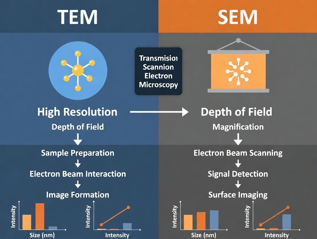
This document provides application notes and protocols for selecting between Transmission Electron Microscopy (TEM) and Scanning Electron Microscopy (SEM) for nanoparticle (NP) characterization. The choice is critical for accurate size, shape, and aggregation state analysis in drug development. This content supports the thesis that an informed selection, and sometimes complementary use, of TEM and SEM is fundamental for robust nanomaterial research. Core differentiators are beam-sample interaction, requisite sample thickness, and the resulting information output.
Quantitative Comparison of Core Physical Parameters
Table 1: Fundamental Operational Differences Between SEM and TEM
| Parameter | Scanning Electron Microscope (SEM) | Transmission Electron Microscope (TEM) |
|---|---|---|
| Beam Type | Focused electron beam scanning the surface. | High-energy, stationary beam transmitted through the sample. |
| Beam Energy Range | Typically 0.1 keV to 30 keV. | Typically 60 keV to 300 keV. |
| Primary Interaction | Interaction with sample surface/near-surface (≤ 1 µm depth). Elastic & inelastic scattering generating secondary/backscattered electrons. | Direct transmission through the sample bulk. Elastic scattering (diffraction) and inelastic scattering (energy loss). |
| Sample Thickness Requirement | Bulk samples, thick coatings. No strict limit; must fit in chamber. | Ultra-thin sections (< 100-200 nm). Nanoparticles typically require support films. |
| Primary Information Output | Topography & Surface Morphology (3D-like image). Elemental composition via EDS. | Internal Structure & Crystallography (2D projection). Lattice imaging, diffraction patterns, core-shell visualization. Elemental mapping via EELS/EDS. |
| Typical Resolution | ~0.5 nm to 5 nm (field emission source). | < 0.1 nm to 1 nm (atomic resolution possible). |
| Sample Preparation Complexity | Low to Moderate. Sputter coating for non-conductive samples. | High. Requires dispersion on TEM grids, potentially microtomy or cryo-fixation for soft materials. |
| Output Image Basis | Signal intensity from emitted electrons mapped to beam scan position. | Direct spatial distribution of transmitted/elastically scattered electrons. |
Table 2: Suitability for Nanoparticle Analysis
| Analysis Goal | Preferred Instrument | Rationale & Output |
|---|---|---|
| Primary Size Distribution | TEM | Direct measurement from projection, unaffected by charging or coating. High resolution discerns true boundaries. |
| Shape & Aspect Ratio | TEM | Unambiguous 2D projection allows precise shape classification (rods, spheres, triangles). |
| Surface Roughness/Topography | SEM | Surface-sensitive signal reveals textural details and 3D morphology. |
| Aggregation State (Dry) | SEM | Excellent for visualizing large-field, 3D aggregate structures on a substrate. |
| Aggregation State (in situ) | TEM (Cryo) | Cryo-TEM preserves hydrated state, showing native dispersion and aggregation. |
| Core-Shell/Layered Structure | TEM | Contrast differences and high-resolution imaging reveal internal architectures. |
| Crystallinity & Lattice Analysis | TEM | Selected Area Electron Diffraction (SAED) and HRTEM provide atomic lattice information. |
Experimental Protocols for Nanoparticle Analysis
Protocol 2.1: SEM Analysis of Nanoparticle Morphology & Aggregation
Objective: To characterize the surface morphology, primary particle size, and dry-state aggregation of synthesized nanoparticles. Materials: See The Scientist's Toolkit. Procedure:
- Sample Preparation: a. Dilute the nanoparticle suspension in appropriate solvent (e.g., water, ethanol) to minimize aggregation. b. Deposit 5-10 µL onto a clean, conductive substrate (e.g., silicon wafer, aluminum stub with conductive tape). c. Allow to air-dry or use a critical point dryer to reduce drying artifacts. d. For non-conductive samples (e.g., polymer NPs), sputter-coat with a 5-10 nm layer of gold/palladium or carbon using a sputter coater to prevent charging.
- Instrument Setup: a. Load sample into the SEM chamber and evacuate. b. Set accelerating voltage (typically 5-20 kV). Use lower kV for surface detail, higher for deeper interaction. c. Select the secondary electron (SE) detector for topography. d. Adjust working distance to 5-10 mm for optimal resolution.
- Imaging & Analysis: a. Navigate to areas of interest at low magnification. b. Acquire high-resolution images at multiple, random fields of view to ensure statistical relevance. c. Use integrated software to measure particle dimensions from calibrated images. Analyze >200 particles for statistical size distribution.
Protocol 2.2: TEM Analysis of Nanoparticle Size, Shape, and Internal Structure
Objective: To determine the primary particle size distribution, shape, and internal crystallographic structure of nanoparticles. Materials: See The Scientist's Toolkit. Procedure:
- Grid Preparation: a. Glow-discharge a TEM grid (e.g., continuous carbon or ultrathin carbon on holey film) to render it hydrophilic.
- Sample Deposition (Negative Stain for non-cryo): a. Dilute nanoparticle suspension to a suitable concentration (often 0.01-0.1 mg/mL). b. Apply 3-5 µL of suspension to the glow-discharged grid and let adsorb for 30-60 seconds. c. Wick away excess liquid with filter paper. d. Immediately apply 3-5 µL of 1-2% aqueous uranyl acetate stain. Incubate for 30 seconds. e. Wick away stain and allow grid to air-dry completely.
- Instrument Setup: a. Load grid into the TEM holder and insert into the column. b. Set accelerating voltage to 80-200 kV. c. Start observation at low magnification to locate suitable, well-dispersed areas.
- Imaging & Diffraction: a. Acquire images at increasing magnifications. Use underfocus (1-2 µm) to enhance phase contrast. b. For size/shape analysis, collect images from multiple grid squares (>200 particles). c. For crystallography, switch to SAED or HRTEM mode. Align the beam and acquire diffraction patterns or lattice images.
- Image Analysis: a. Use software (e.g., ImageJ, proprietary TEM software) to measure particle Feret diameters, aspect ratios, etc., from calibrated images.
Visualization of Decision Workflow and Beam Interactions
Decision Workflow for TEM vs SEM Selection
Comparison of SEM and TEM Beam Interaction Mechanisms
The Scientist's Toolkit: Essential Materials
Table 3: Key Research Reagent Solutions for Nanoparticle EM Analysis
| Item | Function | Typical Specification/Example |
|---|---|---|
| TEM Grids | Support film for nanoparticle deposition. | Copper grids (200-400 mesh) with continuous carbon film (~5-10 nm) or holey carbon film. |
| Negative Stain | Enhances contrast of biological/polymer nanoparticles by embedding in heavy metal salt. | 1-2% Uranyl acetate (aq.) or 2% Phosphotungstic acid (pH 7.0). |
| Conductive Substrates (SEM) | Provides a conductive, flat surface for sample mounting. | Silicon wafers, aluminum SEM stubs with conductive carbon or copper tape. |
| Sputter Coater (SEM) | Applies an ultra-thin conductive metal layer to non-conductive samples to prevent charging. | Gold/Palladium target (80/20), 5-10 nm coating thickness. |
| Glow Discharger | Treats TEM grids to create a hydrophilic surface for even sample spreading. | Low-pressure air or argon plasma treatment for 30-60 seconds. |
| Critical Point Dryer | Removes solvent from samples without surface tension-induced aggregation artifacts. | Uses liquid CO₂; crucial for delicate or hydrated samples before SEM. |
| Particle Analysis Software | Quantifies size, shape, and distribution from acquired micrographs. | ImageJ/FIJI (with plugins), proprietary SEM/TEM software, or standalone packages. |
Within the broader thesis comparing Transmission Electron Microscopy (TEM) and Scanning Electron Microscopy (SEM) for nanoparticle characterization, precise definition of key metrics is fundamental. This application note delineates the core morphological descriptors—size, shape, dispersion, and morphology—critical for robust analysis in drug development and nanomaterials research. Accurate quantification of these parameters underpins the correlation of nanoparticle structure with function, efficacy, and safety.
Defining Core Metrics
| Metric | Quantitative Descriptors | Qualitative Description | Primary TEM/SEM Utility |
|---|---|---|---|
| Size | - Feret's Diameter- Martin's Diameter- Projected Area Diameter- Number-weighted mean (Dn)- Volume-weighted mean (Dv) | The dimensional scale of a particle. For non-spherical particles, size is directionally dependent and must be reported with the measurement method. | TEM: Direct measurement from 2D projection.SEM: Surface topology measurement. |
| Shape | - Aspect Ratio (AR)- Circularity/Sphericity- Roundness- Solidity- Convexity | The geometric form of a particle, independent of its size (e.g., spherical, rod-like, cubic, prismatic). | TEM: High-resolution 2D shape from projection.SEM: 3D surface shape perception. |
| Dispersion | - Polydispersity Index (PDI) from DLS- Coefficient of Variation (CV%)- Span value [(D90-D10)/D50] | The uniformity of size distribution within a population. A monodisperse sample has low variance. | Both: Statistical analysis from population imaging. Critical for counting statistics. |
| Morphology | Combination of size, shape, surface texture, and crystallinity. | The overall visual texture and structure, including surface smoothness/roughness and internal lattice details. | TEM: Ultimate tool for internal morphology/crystallinity.SEM: Superior for surface texture at nano-micro scale. |
Experimental Protocols for Metric Quantification
Protocol 3.1: TEM-Based Size and Shape Analysis
Objective: To obtain number-weighted size distribution and shape factors from nanoparticle projections. Materials: See "Scientist's Toolkit" below. Procedure:
- Sample Preparation: Dilute nanoparticle suspension in appropriate solvent. Deposit 5-10 µL onto a carbon-coated TEM grid. Wick away excess and dry under ambient or controlled atmosphere.
- Imaging: Insert grid into TEM holder. Acquire images at multiple magnifications (e.g., 50kX, 100kX) at low electron dose to prevent beam damage. Capture 10-20 images from different grid squares to ensure statistical significance (>200 particles).
- Image Analysis: a. Import images into analysis software (e.g., ImageJ, Fiji). b. Apply thresholding to create binary masks of nanoparticles. c. Use particle analysis function to measure for each particle: - Area (A) - Feret's Diameter (Max, Min) - Aspect Ratio (Max Feret / Min Feret) - Circularity [4π*(Area) / (Perimeter)^2] d. Export data to statistical software. Calculate Dn, Dv, PDI (as CV%), and mean Aspect Ratio.
Protocol 3.2: SEM-Based Morphology and Dispersion Analysis
Objective: To characterize surface morphology and assess population dispersion. Procedure:
- Sample Preparation: For dry powders, use adhesive carbon tape on an aluminum stub. For suspensions, deposit and dry on a silicon wafer. Sputter-coat with 5-10 nm of Au/Pd if the material is non-conductive.
- Imaging: Insert stub into SEM chamber. Evacuate. Use accelerating voltage of 5-15 kV. Acquire secondary electron (SE) images at various magnifications. Use tilting to appreciate 3D shape.
- Analysis: a. For size/dispersion: Follow steps similar to Protocol 3.1, noting that sizes are surface-topological. b. For morphology: Qualitatively describe surface features (smooth, porous, rough, faceted). Use image contrast to infer topographic details.
Visualizing the Analysis Workflow
TEM/SEM Analysis Workflow
The Scientist's Toolkit: Essential Materials
| Item | Function | Example/Note |
|---|---|---|
| Carbon-coated TEM Grids | Support film for nanoparticle deposition, provides conductivity and low background. | Copper, 300-400 mesh. |
| Ultra-sonicator | Disperses aggregates in suspension prior to grid deposition. | Critical for accurate size analysis. |
| Precision Micropipettes | Accurate deposition of sample volume onto TEM grid. | 2-20 µL range. |
| Sputter Coater | Applies thin conductive metal layer (Au, Au/Pd, Cr) for non-conductive SEM samples. | Reduces charging, improves SE yield. |
| SEM Sample Stubs | Holds sample in SEM chamber. | Aluminum with adhesive carbon tape. |
| Image Analysis Software | Quantifies particle parameters from micrographs. | ImageJ/Fiji (open source), commercial packages. |
| Statistical Software | Calculates population statistics (mean, SD, PDI, distributions). | Origin, GraphPad Prism, Python/R. |
Step-by-Step Protocols: Sample Prep, Imaging, and Analysis for TEM and SEM
Within the broader thesis comparing Transmission Electron Microscopy (TEM) and Scanning Electron Microscopy (SEM) for nanoparticle (NP) analysis, sample preparation is the critical differentiator. TEM provides superior resolution for internal structure and sub-nanometer shape detail but demands more stringent and artifact-prone preparation. This application note details key TEM protocols, highlighting how preparation choices directly impact data fidelity in comparative NP characterization studies.
Grid Selection for TEM Analysis
The choice of support grid is foundational. Incorrect selection leads to poor sample adherence, grid-specific artifacts, and compromised imaging.
Research Reagent Solutions: TEM Grids
| Item | Function & Key Characteristics |
|---|---|
| Copper Mesh Grids | Most common; cost-effective; conductive. Unsuitable for acidic or metal-sensitive samples. |
| Gold Mesh Grids | Inert; essential for biological samples or when corrosion is a concern. |
| Holey/Carbon Film Grids | Continuous carbon over holes provides support for cryo-EM; allows particles to span holes, minimizing background. |
| Lacey Carbon Grids | Irregular lacey network ideal for isolating particles over thin carbon edges. |
| Formvar/Carbon-Coated Grids | Plastic (Formvar) film coated with carbon provides a stable, continuous support film for general NP analysis. |
| UltraFoil Gold Grids | Gold foil with no carbon film; minimal background for high-resolution cryo-TEM and EDS. |
Table 1: Common TEM Grid Specifications
| Grid Type | Mesh Size | Primary Coating | Best For | Key Limitation |
|---|---|---|---|---|
| Copper, Square | 200-400 | Formvar/Carbon | Routine negative stain, general NP | Sample-grid interactions |
| Copper, Hexagonal | 300 | Holey Carbon | Cryo-TEM, high-res | Fragile, requires glow discharge |
| Gold, Square | 200 | Lacey Carbon | Sensitive/biological NPs | High cost |
| Nickel, Square | 200 | Continuous Carbon | Elemental Analysis (EDS) | Magnetic, can interfere |
Detailed Protocol: Negative Staining for Rapid NP Assessment
Principle: Surround NPs with a heavy metal salt (stain) to create a negative image, enhancing contrast. Ideal for quick shape/size checks in thesis comparative work.
Materials: Uranyl acetate (2%) OR ammonium molybdate (2%); Parafilm; Filter paper; Glow discharger; Forceps.
Detailed Methodology:
- Grid Activation: Subject a Formvar/carbon-coated copper grid (300 mesh) to a low-pressure glow discharge for 30-45 seconds to render it hydrophilic.
- Sample Application: Pipette 5-10 µL of purified NP suspension (optimal concentration ~0.1 mg/mL) onto the grid. Incubate for 1 minute.
- Blotting: Gently wick away excess liquid using the edge of a filter paper. Do not let the grid dry completely.
- Staining: Immediately apply 10 µL of stain (e.g., 2% uranyl acetate). Incubate for 30-60 seconds.
- Wash & Dry: Blot the stain, then briefly touch the grid to a droplet of deionized water (if using uranyl acetate) to wash. Blot thoroughly. Air-dry for 5 minutes before TEM insertion.
Detailed Protocol: Cryo-TEM for Native-State Hydrated NPs
Principle: Vitrify NP suspension to preserve native hydration state and prevent drying artifacts. Gold standard for in-situ shape/size analysis in thesis.
Materials: Cryo-TEM grid (Quantifoil Au 300 R1.2/1.3); Vitrobot or manual plunger; Ethane slush; Liquid Nitrogen; Filter paper.
Detailed Methodology:
- Grid Preparation: Glow discharge the cryo-grid under hydrophilic conditions.
- Vitrobot Setup: Set chamber to 100% humidity and 4°C (or room temp for stable NPs). Pre-wet blotting paper.
- Loading & Blotting: Apply 3 µL of NP sample to the grid inside the chamber. Initiate automated blotting (blot force: 0, blot time: 3-6 seconds) to create a thin film (~100 nm).
- Plunging & Vitrification: Immediately plunge the grid into liquid ethane cooled by liquid nitrogen. Hold for >5 seconds.
- Storage: Transfer grid under liquid nitrogen to a cryo-grid box and store in a dewar until TEM imaging (using a cryo-holder at <-170°C).
Table 2: Impact of Sample Prep Method on NP Measurement (Thesis Context)
| Preparation Method | Estimated Size Inflation | Preserves Hydration? | Typical Artifacts | Best for Thesis Use Case |
|---|---|---|---|---|
| Negative Stain | +10-20% (stain shell) | No | Stain granularity, aggregation | Rapid screening, shape confirmation vs. SEM |
| Cryo-TEM | Minimal (<2%) | Yes | Beam-induced motion, vitrification cracks | Absolute size/shape benchmark vs. SEM & DLS |
| Air Drying | +15-50% (flattening) | No | Flattening, aggregation, meniscus effects | Artifact study (what to avoid) |
| Critical Point Drying | +5-15% | No | Residual shrinkage, structural collapse | Less common for primary NP analysis |
Drying Artifacts: Identification and Mitigation
Artifacts from drying are the primary source of discrepancy between TEM and SEM size measurements in a thesis.
Common Artifacts:
- Flattening/Spreading: NPs appear larger and flattened on the substrate. Mitigation: Use cryo-TEM or quick-freeze/deep-etch.
- Aggregation & Meniscus Effects: NPs pile at droplet edges during drying. Mitigation: Use controlled humidity blotting (Vitrobot), add surfactants cautiously.
- Salt Crystals: Residual buffers form crystalline structures. Mitigation: Dialyze into volatile buffers (e.g., ammonium acetate), use grid washing steps.
Table 3: Artifact Comparison: TEM vs. SEM
| Artifact Type | Manifestation in TEM | Manifestation in SEM | Primary Mitigation Strategy |
|---|---|---|---|
| Charging | Beam deflection, image drift | Bright streaks, abnormal contrast | Conductive coating (SEM), thin carbon support (TEM) |
| Dehydration | Collapse, flattening | Shrinkage, cracking | Cryo-preparation (both), CPD (SEM) |
| Aggregation | Clusters misinterpreted as large particles | Similar clustering | Improved dispersion pre-application |
| Substrate Interaction | Altered shape at contact point | Less pronounced due to coating | Use inert grids (Au), functionalized surfaces |
Visualization: TEM Sample Preparation Decision Pathway
Decision Tree for TEM Sample Preparation
Visualization: Cryo-TEM Workflow for Nanoparticles
Cryo-TEM Sample Vitrification Workflow
Within the broader thesis comparing Transmission Electron Microscopy (TEM) and Scanning Electron Microscopy (SEM) for nanoparticle size and shape analysis, SEM sample preparation is a critical variable. While TEM offers superior resolution for internal structure, SEM provides excellent topographical and compositional data with greater depth of field and easier sample preparation for many materials. However, SEM analysis of sensitive materials, such as organic nanoparticles, liposomes, or biological drug carriers, presents unique challenges. These samples are often non-conductive, beam-sensitive, and hydrated, leading to charging artifacts, thermal degradation, and structural collapse under the electron beam. This application note details refined protocols for substrate mounting, conductive coating, and the use of low-vacuum mode to enable accurate SEM characterization of sensitive nanomaterials, directly contributing to robust comparative analyses in nanomedicine research.
Key Challenges & Comparative Data
Table 1: Primary Challenges in SEM Analysis of Sensitive Nanoparticles
| Challenge | Consequence for SEM Imaging | Impact on Comparison with TEM |
|---|---|---|
| Electron Charging | Bright streaks, image distortion, beam deflection. | Overestimates particle size, obscures shape; TEM less affected in cryo-mode. |
| Thermal Damage | Melting, bubbling, decomposition of particles. | Alters native morphology; TEM at low dose can better preserve structure. |
| Low Volatility | Contamination of column in high vacuum. | Requires specialized SEM modes; TEM requires high vacuum always. |
| Low Atomic Number | Poor secondary electron yield, weak signal. | Low image contrast; TEM offers mass-thickness contrast. |
Table 2: SEM Preparation Strategies for Sensitive vs. Robust Materials
| Parameter | Standard Inorganic Nanoparticles | Sensitive Organic/Biological Nanoparticles |
|---|---|---|
| Substrate | Standard conductive tape, silicon wafer. | Freshly glow-discharged carbon-coated grids, conductive agarose, or poly-L-lysine coated substrates. |
| Mounting Adhesive | Carbon paste, silver paint. | Ultrapure water or buffer for adsorption; minimal, dilute adhesives. |
| Drying Method | Air drying, oven. | Critical point drying, freeze-drying, or solvent-exchange drying. |
| Conductive Coating | Sputter coating with 10-20 nm Au/Pd. | Ultra-thin (2-5 nm) coating of Au/Pd or Cr; or non-coating using LV-SEM. |
| Microscope Mode | High Vacuum (HV), 5-30 kV. | Low Vacuum (LV-ESEM) or Variable Pressure (VP-SEM), 1-15 kV. |
Detailed Experimental Protocols
Protocol 3.1: Substrate Mounting for Sensitive Nanoparticles
Objective: To immobilize nanoparticles without aggregation or structural alteration. Materials: See "The Scientist's Toolkit" (Section 6). Procedure:
- Substrate Preparation: Use a 5x5 mm silicon chip or a glass coverslip. Clean ultrasonically in ethanol for 5 minutes and dry under nitrogen.
- Surface Functionalization (Optional): To improve adhesion, treat the substrate with 0.1% w/v poly-L-lysine for 10 minutes. Rinse gently with deionized water and air dry.
- Sample Application: Dilute the nanoparticle suspension in its native buffer (e.g., 10 mM HEPES) to an appropriate concentration (OD ~0.1). Pipette 5-10 µL onto the substrate.
- Adsorption: Allow adsorption for 15-20 minutes in a humid chamber to prevent evaporation artifacts.
- Rinsing: Gently rinse the substrate with 2-3 drops of ultrapure water or volatile buffer (e.g., ammonium acetate) to remove salts and non-adsorbed material. Blot, do not wipe.
- Drying: Proceed immediately to Critical Point Drying (CPD) or freeze-drying.
- CPD Method: Dehydrate sample through an ethanol series (30%, 50%, 70%, 90%, 100%, 100%; 5 min each). Transfer to CPD chamber, purge with liquid CO₂, and execute the critical point cycle.
- Freeze-Drying Method: Snap-freeze the rinsed sample in liquid nitrogen slush. Transfer to a pre-cooled freeze-dryer and lyophilize for 12-24 hours.
Protocol 3.2: Ultra-Thin Conductive Coating via Sputter Coating
Objective: To apply a minimal, continuous conductive layer to prevent charging while preserving fine surface details. Materials: Sputter coater with planetary tilt stage, Au/Pd (80/20) target, chromium target. Procedure:
- Load the dried sample from Protocol 3.1 onto the coater stage. Ensure the stage is at its maximum distance from the target.
- Evacuate the chamber to a base pressure of ≤ 5 x 10⁻² mbar.
- For Au/Pd coating: Set current to 20 mA. Introduce Ar gas to a working pressure of 0.05 mbar. Use a planetary rotation stage. Coat for 30-45 seconds, resulting in an approximate 2-3 nm film.
- For Chromium coating (better adhesion for organic materials): Use a DC magnetron. Set power to 50W. Coat for 15-20 seconds for a ~2 nm film.
- Vent the chamber and remove the sample. Store in a desiccator until SEM analysis.
Protocol 3.3: Imaging in Low-Vacuum (Variable Pressure) Mode
Objective: To image uncoated, sensitive samples by mitigating charge build-up using a gaseous environment. Materials: VP-SEM or ESEM capable microscope. Procedure:
- Mount the uncoated or thinly coated sample on a standard SEM stub using double-sided carbon tape.
- Insert the sample into the VP-SEM chamber. Do not use a standard high-vacuum stage if incompatible.
- Set Chamber Conditions: Pump the chamber to a level of ~0.5 torr (70 Pa). Introduce water vapor (for ESEM) or nitrogen gas as the imaging gas. The gas molecules become ionized by stray electrons, neutralizing charge on the sample surface.
- Microscope Parameters: Reduce accelerating voltage to 5-10 kV. Use a backscattered electron (BSE) detector or a dedicated gaseous secondary electron (GSE) detector. The BSE detector is less sensitive to the gas environment.
- Optimization: Adjust the chamber pressure (typically 0.1-2.0 torr) and voltage iteratively to find the best contrast while eliminating charging (no image drift or bright flashes).
Workflow & Decision Pathways
SEM Sample Prep Decision Pathway for Sensitive Materials
Table 3: Impact of Preparation Method on Measured Nanoparticle Size (Hypothetical Data)
| Preparation Method | Average Size (nm) | Standard Deviation (nm) | Observed Morphology | Likely Artifact Introduced |
|---|---|---|---|---|
| Air Dried, Uncoated (HV-SEM) | 152 | 45 | Aggregated, Flattened | Dehydration flattening, charging |
| Air Dried, 10nm Au/Pd (HV-SEM) | 125 | 25 | Distinct, Slightly enlarged | Coating thickness overestimation |
| Critical Point Dried, 3nm Cr (HV-SEM) | 102 | 12 | Spherical, Well-defined | Minimal |
| Uncoated, LV-SEM (1 torr H₂O) | 98 | 15 | Spherical, Some edge fuzziness | Gas scattering reduces resolution |
| Cryo-TEM (Reference) | 95 | 8 | Spherical, Uniform | Accepted as nearest to native state |
The Scientist's Toolkit
Table 4: Essential Research Reagent Solutions & Materials
| Item | Function & Rationale |
|---|---|
| Poly-L-lysine solution (0.1% w/v) | A cationic polymer that coats negatively charged substrates (e.g., silicon, glass), improving adhesion of a wide range of nanoparticles via electrostatic interaction. |
| Ultrapure Water (HPLC grade) | Used for final rinsing to remove crystalline salts that create artifacts upon drying. Low conductivity prevents unwanted reactions. |
| Ethanol Series (30%, 50%, 70%, 90%, 100%) | For gradual dehydration of hydrated samples prior to Critical Point Drying, minimizing structural collapse from surface tension. |
| Liquid Nitrogen Slush | Provides rapid, uniform freezing for freeze-drying or cryo-preparation, vitrifying water to reduce ice crystal damage. |
| Au/Pd (80/20) Target | Sputter coating target alloy. Provides a fine-grained, conductive layer with lower mobility than pure gold, offering better detail preservation. |
| Chromium Target | Provides an ultra-thin, highly adherent coating for organic materials, ideal as a seed layer before a light noble metal coat. |
| Conductive Carbon Tape | Standard mounting adhesive. Provides a conductive path from sample to stub, crucial for charge dissipation in HV-SEM. |
| Double-Sided Adhesive Discs | For mounting delicate, dried samples without the risk of smearing associated with carbon paste. |
| Silicon Wafer Chips | An ultra-flat, clean, and easily functionalized substrate. Semiconducting nature reduces charging for uncoated imaging at low kV. |
| HEPES Buffer (10 mM, pH 7.4) | A non-volatile, biological buffer for sample dilution and rinsing that maintains nanoparticle stability and is relatively clean under SEM. |
Within the context of a broader thesis comparing Transmission Electron Microscopy (TEM) and Scanning Electron Microscopy (SEM) for nanoparticle size and shape analysis, optimizing imaging parameters is critical. For applications in drug development, such as characterizing lipid nanoparticles or viral vectors, achieving optimal contrast is essential for accurate quantification. This application note provides detailed protocols and data for selecting Accelerating Voltage (kV), Magnification, and Detector type to maximize contrast for different sample types.
Table 1: Recommended Parameters for Common Nanoparticle Types
| Nanoparticle Type | Preferred Instrument | Optimal Accelerating Voltage (kV) | Typical Magnification Range | Recommended Detector for Contrast | Rationale |
|---|---|---|---|---|---|
| Polymer-based NPs (e.g., PLGA) | TEM | 80-120 kV | 50,000x - 150,000x | In-column Energy Filter (IF) or Slow-scan CCD | Reduces charging, enhances mass-thickness contrast. |
| Metallic NPs (e.g., Gold, Silver) | TEM | 120-200 kV | 100,000x - 300,000x | High-Angle Annular Dark Field (HAADF) STEM | Z-contrast is dominant; minimizes diffraction effects. |
| Lipid NPs / Liposomes | Cryo-TEM | 120-200 kV (Low dose) | 30,000x - 80,000x | Direct Electron Detector (DED) | Maximizes signal-to-noise for beam-sensitive, low-contrast samples. |
| Surface Topography of Aggregates | SEM | 1-5 kV (LV) | 50,000x - 100,000x | In-lens SE Detector | Enhances surface detail, reduces penetration volume. |
| Size Distribution in a Matrix | SEM | 10-15 kV | 20,000x - 50,000x | Backscattered Electron (BSE) with YAG crystal | Optimizes atomic number contrast against organic background. |
Table 2: Impact of Accelerating Voltage on Image Parameters
| Accelerating Voltage | Electron Wavelength | Sample Penetration | Beam Damage Risk | Typical Contrast Outcome |
|---|---|---|---|---|
| 5 kV (SEM) | 0.173 Å | Very Low (nm scale) | Low (surface only) | High surface topography contrast. |
| 20 kV (SEM) | 0.085 Å | Moderate (µm scale) | Medium | Balance of surface and bulk information. |
| 80 kV (TEM) | 0.0418 Å | High for thin samples | Medium-High | Good contrast for organic materials. |
| 200 kV (TEM) | 0.0251 Å | Very High | High (for sensitive samples) | High resolution, lower scattering contrast for light elements. |
Experimental Protocols
Protocol 3.1: Optimizing TEM Contrast for Polymer Nanoparticles
Objective: Achieve size and shape analysis of poly(lactic-co-glycolic acid) (PLGA) nanoparticles with sub-2 nm precision. Materials: See "Scientist's Toolkit" (Section 5). Procedure:
- Sample Prep: Apply 5 µL of diluted NP suspension onto a glow-discharged, carbon-coated TEM grid. Blot after 60 sec and stain with 1% uranyl acetate for 45 sec. Air-dry.
- Microscope Setup: Insert grid into TEM (e.g., JEOL JEM-1400Plus). Start at 80 kV.
- Low Mag Survey: Use 5,000x magnification with a CCD camera to locate suitable, thin areas of the support film.
- Voltage Test: At 50,000x, acquire images at 80 kV, 100 kV, and 120 kV. Note the contrast and integrity of particles.
- Detector Comparison: At the optimal voltage (typically 100 kV), acquire images using:
- Bright-Field (BF) TEM: Near focus, slight underfocus (~1 µm) to enhance phase contrast.
- Dark-Field (DF) TEM: Tilting beam to select scattered electrons.
- High-Resolution Imaging: Zoom to 120,000x. Use a slow-scan CCD or a CMOS camera with an exposure time of 1-2 sec. Employ low-dose mode if available.
- Analysis: Measure particle diameter using ImageJ software (≥100 particles).
Protocol 3.2: SEM Imaging for Topographical and Compositional Contrast
Objective: Distinguish gold nanoparticle aggregates from a proteinaceous background. Materials: See "Scientist's Toolkit" (Section 5). Procedure:
- Sample Prep: Sputter-coat sample with 5 nm of carbon (not metal) to ensure conductivity while preserving BSE signal.
- Microscope Setup: Use a field-emission SEM (e.g., Zeiss Gemini). Begin at 5 kV, using the In-lens SE detector.
- Topography Imaging: At 10,000x, fine-tune voltage (1-5 kV) to highlight aggregate edges without charging.
- Switch to BSE Mode: Increase voltage to 10 kV. Switch to the BSE detector (e.g., solid-state 4-quadrant).
- Optimize Contrast/Composition:
- Tilt stage to 0° (normal).
- Adjust detector contrast and brightness to maximize intensity difference between high-Z (gold, bright) and low-Z (protein, dark) regions.
- Combined Imaging: Use software mixing to overlay SE and BSE signals (e.g., 30% SE, 70% BSE) for simultaneous topographical and compositional information.
- Automated Mapping: For large areas, use automated stage and software to acquire multiple BSE images for aggregate counting.
Diagrams
Decision Workflow for TEM/SEM Imaging Parameter Selection
TEM and SEM Signal Paths and Contrast Mechanisms
The Scientist's Toolkit: Key Research Reagent Solutions
Table 3: Essential Materials for Nanoparticle EM Imaging
| Item | Function & Rationale | Example Product/Brand |
|---|---|---|
| Glow Discharger | Creates a hydrophilic, negatively charged surface on TEM grids, ensuring even sample spread and adhesion. | PELCO easiGlow |
| Carbon-Coated TEM Grids | Provide an ultrathin, conductive, and amorphous support film, minimizing background interference. | Ted Pella Lacey Carbon, 400 mesh Cu |
| Negative Stain (Uranyl Acetate) | Surrounds particles, increasing mass-thickness contrast in TEM by scattering electrons away from the particle edges. | 1-2% aqueous solution (note: radioactive, handle with care) |
| Cryo-Plunger | Vitrifies aqueous nanoparticle suspensions in a thin layer of amorphous ice for native-state Cryo-TEM imaging. | Thermo Fisher Scientific Vitrobot Mark IV |
| Conductive Carbon Tape | Provides a reliable, low-outgassing electrical contact for SEM samples, reducing charging artifacts. | Ted Pella Double-Sided Carbon Tape |
| Sputter Coater with Carbon Rod | Applies an ultra-thin (3-10 nm), uniform conductive carbon layer for SEM BSE imaging, preserving compositional data. | Quorum Q150T ES |
| Reference Nanoparticles | Gold or polystyrene beads of known size (e.g., 10 nm, 100 nm) for microscope calibration and size validation. | BBI Solutions Gold Nanoparticles, NIST Traceable |
| Lowicryl or EPON Resin | For embedding nanoparticles for ultramicrotomy, allowing cross-sectional analysis in TEM. | Sigma-Aldrich Embedding Kits |
Application Notes
Within a comprehensive thesis comparing Transmission Electron Microscopy (TEM) and Scanning Electron Microscopy (SEM) for nanoparticle characterization in drug development, the method of image analysis is a critical variable. Manual and automated Particle Size Distribution (PSD) analysis offer distinct advantages and limitations, directly impacting the accuracy, reproducibility, and throughput of data derived from both TEM and SEM micrographs.
For TEM, which provides high-resolution 2D projections of nanoparticles, manual analysis can be essential for complex, aggregated, or non-spherical particles where software algorithms may fail in proper boundary detection. However, it is subjective and time-consuming. Automated analysis offers high-throughput, unbiased measurement but requires high-contrast, well-dispersed samples and careful threshold calibration to avoid artifacts like under- or over-segmentation.
For SEM, which provides 3D surface topography, manual analysis is often used to distinguish nanoparticles from substrate texture. Automated analysis of SEM images benefits from depth information but is challenged by shadowing and charging effects. The choice between manual and automated PSD must be aligned with the microscope's output, the sample's nature, and the study's requirements for statistical power and regulatory compliance (e.g., FDA guidelines for nanomedicine).
Table 1: Comparison of Manual vs. Automated PSD Analysis
| Parameter | Manual Analysis | Automated Analysis |
|---|---|---|
| Throughput | Low (50-100 particles/hour) | Very High (1000+ particles/minute) |
| Objectivity | Low (Prone to user bias) | High (Algorithm-driven) |
| Reproducibility | Moderate to Low (High inter-operator variability) | High (Consistent with same parameters) |
| Best For | Complex shapes, low contrast, aggregated samples, small sample sizes (N < 300) | Spherical/monodisperse samples, high-throughput, large N for statistics (N > 1000) |
| Key Software Tools | ImageJ/Fiji (with manual overlay), Adobe Photoshop | ImageJ (Particle Analyzer), Malvern IPS, Nikon NIS-Elements, AI-based platforms (Ilastik) |
| Typical Coefficient of Variance (Repeatability) | 8-15% | 2-5% (with optimized settings) |
| Regulatory Acceptance | Often requires stringent SOPs and multiple analysts | Favored for its consistency and audit trail |
Table 2: PSD Output Discrepancy Between TEM & SEM (Hypothetical Gold Nanoparticle Sample)
| Analysis Method | TEM Mean Size (nm) ± SD | SEM Mean Size (nm) ± SD | Notes on Discrepancy |
|---|---|---|---|
| Manual (n=200) | 24.5 ± 3.2 | 26.1 ± 3.8 | SEM measures surface topology; slight overestimation possible due to coating or edge effect. |
| Automated (n=10,000) | 23.8 ± 2.9 | 25.4 ± 3.5 | Automated analysis confirms trend with greater statistical confidence. |
| Reported PDI (from DLS) | 0.08 | 0.08 | PDI from DLS correlates better with automated, high-N image analysis. |
Experimental Protocols
Protocol 1: Manual PSD Analysis from TEM/SEM Micrographs
Objective: To determine the size distribution of nanoparticles by manual measurement, minimizing bias.
Materials: See "The Scientist's Toolkit" below.
Procedure:
- Image Acquisition: Capture a minimum of 10 representative micrographs from different grid/sample areas at consistent magnification (e.g., 80,000x for TEM, 50,000x for SEM). Ensure scale bar is embedded.
- Calibration: Open the image in ImageJ/Fiji. Use the straight-line tool to measure the scale bar. Set
Analyze > Set Scaleto input the known distance and unit. - Measurement Setup: Set measurements (
Analyze > Set Measurements) to includeArea,Feret's diameter(for maximum dimension), andShape descriptors. - Manual Tracing:
- Use the oval or polygon selection tool to carefully trace the perimeter of each particle. For non-spherical particles, use Feret's diameter or trace the area for equivalent circular diameter calculation.
- Avoid measuring particles at the extreme edges, those that are clearly aggregated, or those out of focus.
- Press
Ctrl+M(Cmd+M on Mac) to record the measurement for each particle.
- Data Collection: Aim for a minimum of 200-300 particles per sample for a statistically relevant distribution. Record all data in the built-in Results window.
- Data Export & Analysis: Export results to a CSV file. Calculate mean, standard deviation, and generate a histogram in statistical software (e.g., Excel, Prism).
Protocol 2: Automated PSD Analysis Using ImageJ/Fiji
Objective: To perform high-throughput, reproducible particle size analysis from high-contrast micrographs.
Procedure:
- Image Preparation: Acquire images as in Protocol 1. Pre-process images if necessary: convert to 8-bit (
Image > Type > 8-bit), and apply background subtraction (Process > Subtract Background, rolling ball radius ~50 pixels). - Thresholding (Critical Step): Convert the image to a binary mask. Use
Image > Adjust > Threshold. Adjust the sliders so that particles are accurately selected (appear red) without merging or including noise. Use auto-thresholding methods (e.g., Otsu, Intermodes) consistently across all images. - Binary Processing: Clean the binary mask:
Process > Binary > Watershedto separate touching particles. Remove small noise withProcess > Binary > Remove Outliers. - Particle Analysis: Run
Analyze > Analyze Particles. Set a reasonable size range (e.g., 10-Infinity nm²) and circularity (0.5-1.0) to exclude debris. CheckDisplay results,Summarize, andAdd to Manager. - Validation: Visually inspect the overlay of particle outlines on the original image. Manually verify a subset for accuracy. Adjust threshold and re-run if necessary.
- Batch Processing: For multiple images, use the
Process > Batch > Macrofunction with a recorded macro of steps 1-5.
Protocol 3: Cross-Validation Workflow for TEM/SEM Thesis Research
Objective: To systematically compare nanoparticle size data obtained from TEM, SEM, and orthogonal techniques (e.g., DLS).
Procedure:
- Sample Preparation: Split a single, homogenized nanoparticle suspension (e.g., liposomal drug product) for TEM (negative stain, grid), SEM (conductive coating, stub), and DLS analysis.
- Parallel Imaging & Analysis: Perform TEM and SEM imaging on the same day under optimized conditions. Analyze each set of images using both Manual (Protocol 1) and Automated (Protocol 2) methods, performed by separate analysts.
- Data Consolidation: Compile all mean diameters and size distributions into a master table (see Table 2 format).
- Statistical Comparison: Perform a one-way ANOVA or t-test to determine if significant differences (p < 0.05) exist between the means from TEM-Manual, TEM-Auto, SEM-Manual, and SEM-Auto.
- Method Decision: Based on throughput needs, particle complexity, and statistical agreement with DLS, select the optimal microscopy-analysis combination for the remainder of the thesis study.
Visualizations
Title: Cross-Validation Workflow for Nanoparticle Sizing
Title: Decision Tree for Manual vs Automated PSD
The Scientist's Toolkit
Table 3: Essential Research Reagent Solutions & Materials for PSD Analysis
| Item | Function in PSD Analysis |
|---|---|
| TEM Grids (Carbon-coated, e.g., Quantifoil) | Provide an ultrathin, conductive support film for nanoparticle deposition in TEM imaging. |
| SEM Specimen Stubs (Aluminum) & Conductive Tape | Mount non-conductive samples for SEM; tape provides adhesion and electrical path to reduce charging. |
| Negative Stain (2% Uranyl Acetate or Phosphotungstic Acid) | Enhances contrast of biological nanoparticles (e.g., liposomes, viruses) in TEM by enveloping them. |
| Sputter Coater (Gold/Palladium) | Applies a thin conductive metal layer to non-conductive samples for SEM to prevent charging artifacts. |
| ImageJ/Fiji Software (Open Source) | Core platform for both manual and automated image analysis; hosts essential plugins for PSD. |
| Reference Material (NIST Traceable Nanosphere Standards, e.g., 100nm polystyrene) | Calibrates both SEM/TEM magnification and validates the accuracy of PSD analysis workflows. |
| Statistical Software (e.g., GraphPad Prism, OriginPro) | Analyzes size distribution data, performs statistical tests, and generates publication-quality graphs. |
Thesis Context: TEM vs. SEM for Nanoparticle Analysis
Within the broader thesis comparing Transmission Electron Microscopy (TEM) and Scanning Electron Microscopy (SEM) for nanoparticle characterization, this document highlights specific, advanced applications. While TEM excels in internal structural resolution (e.g., lipid bilayers) and SEM in topographical surface detail (e.g., porosity), combined correlative approaches provide a holistic morphological analysis critical for modern nanomedicine development.
Application Note 1: TEM for Liposome Bilayer Imaging
Objective: To resolve the lamellar structure of liposomal bilayers, measure bilayer thickness, and assess structural integrity for drug encapsulation quality control.
Key Quantitative Data (Liposome Bilayer Analysis):
| Parameter | Typical Value Range (DOPC Liposomes) | Instrumentation (TEM) | Sample Prep Method |
|---|---|---|---|
| Bilayer Thickness | 4.0 - 5.5 nm | Cryo-TEM, High-Resolution TEM | Negative Stain, Cryo-Fixation |
| Liposome Diameter | 50 - 200 nm | TEM with CCD camera | Freeze-Fracture (for size dist.) |
| Number of Lamellae | 1 (Unilamellar) to 5+ (Multilamellar) | High-Resolution TEM | Cryo-Fixation |
| Membrane Distortion | Qualitative Assessment (Present/Absent) | TEM at 80-120 kV | Negative Stain (e.g., UA) |
Detailed Protocol: Negative Staining TEM for Liposome Bilayer Visualization
Sample Preparation:
- Dilute liposome suspension (e.g., DOPC:Cholesterol 55:45 mol%) to 0.1 mg/mL lipid concentration in appropriate buffer (e.g., 10 mM HEPES, 150 mM NaCl, pH 7.4).
- Apply a 5-10 µL aliquot of the diluted suspension onto a glow-discharged carbon-coated copper TEM grid for 60 seconds.
- Blot excess liquid with filter paper from the grid edge.
Negative Staining:
- Immediately apply a 5-10 µL drop of 2% (w/v) aqueous uranyl acetate solution onto the grid. Incubate for 60 seconds.
- Blot off the stain thoroughly and allow the grid to air-dry completely (~5 minutes).
Imaging & Analysis:
- Insert grid into TEM (e.g., JEOL JEM-1400Plus) operated at 80-120 kV.
- Acquire images at magnifications of 40,000x to 100,000x.
- Use image analysis software (e.g., ImageJ) to measure bilayer thickness perpendicular to the membrane plane at multiple points, averaging results.
Diagram Title: TEM Liposome Sample Preparation and Analysis Workflow
Application Note 2: SEM for Microparticle Surface Porosity
Objective: To characterize the surface porosity, pore size distribution, and surface roughness of polymeric microparticles (e.g., PLGA) used for controlled drug release.
Key Quantitative Data (Microparticle Porosity Analysis):
| Parameter | Typical Value Range (PLGA Microparticles) | Instrumentation (SEM) | Analysis Software |
|---|---|---|---|
| Average Pore Diameter | 50 - 500 nm | Field-Emission SEM (FE-SEM) | ImageJ, Fiji with Porosity Plugin |
| Surface Porosity (%) | 20 - 60% | FE-SEM at 5-10 kV | Thresholding & Binary Analysis |
| Particle Diameter | 1 - 50 µm | Low-Vacuum SEM | Direct measurement from SEM images |
| Surface Roughness (Qual.) | Smooth, Pitted, Rugose | FE-SEM, Tilt Imaging | Qualitative Comparison |
Detailed Protocol: SEM Imaging of Microparticle Surface Porosity
Sample Mounting:
- Adhere double-sided conductive carbon tape firmly to an aluminum SEM stub.
- Gently sprinkle dry microparticle powder onto the tape. Invert stub and tap to remove loose, non-adherent particles.
Sputter Coating:
- Place the stub in a sputter coater (e.g., Quorum Q150R ES).
- Coat the sample with a 10-15 nm layer of gold/palladium (Au/Pd) under argon atmosphere to ensure surface conductivity.
Imaging & Analysis:
- Insert the coated stub into an FE-SEM (e.g., Zeiss Sigma 500).
- Operate at an accelerating voltage of 5-10 kV and a working distance of 5-10 mm.
- Capture secondary electron (SE) images at various magnifications (e.g., 5,000x, 20,000x, 50,000x).
- For porosity analysis, import images into ImageJ. Convert to 8-bit, adjust threshold to isolate pores, and run "Analyze Particles" to determine pore count, size, and area percentage (porosity).
Diagram Title: SEM Microparticle Porosity Characterization Workflow
Application Note 3: Combined Correlative Microscopy Approaches
Objective: To integrate TEM and SEM data from the same or sister samples for comprehensive particle characterization, linking internal nanostructure (TEM) to external surface morphology (SEM).
Key Quantitative Data (Correlative Analysis):
| Analysis Goal | TEM Contribution | SEM Contribution | Combined Insight |
|---|---|---|---|
| Structure-Porosity Link | Core-shell thickness, lamellarity | Pore density on surface | Effect of formulation on drug release kinetics. |
| Defect Analysis | Internal void detection | Surface crack imaging | Identification of manufacturing failure points. |
| 3D Reconstruction | 2D slice internal details | Surface topography for alignment | Pseudo-3D model of particle architecture. |
Detailed Protocol: Sequential SEM-TEM Analysis on Similar Batches
Sample Division & Parallel Preparation:
- Split a single batch of nanoparticles/microparticles into two representative aliquots.
- Prepare Aliquot A for SEM per the protocol above (sputter-coated on a stub).
- Prepare Aliquot B for TEM per the relevant protocol (stained on a grid).
Correlative Imaging Strategy:
- SEM First: Image Aliquot A with FE-SEM to document surface features, porosity, and overall particle morphology. Capture low-mag maps to locate regions of interest.
- TEM Follow-up: Image Aliquot B with TEM/STEM to resolve internal structures (e.g., bilayer, crystalline drug domains, core-shell interface).
Data Integration:
- Use particle size distributions from both techniques to validate measurements.
- Correlate the presence of surface pores (SEM) with localized thinning or defects in the internal membrane/wall (TEM).
- Combine datasets to build a more complete model explaining functional performance (e.g., burst release linked to both surface pore size and shell thickness).
Diagram Title: Combined SEM and TEM Correlative Analysis Strategy
The Scientist's Toolkit: Key Research Reagent Solutions
| Item Name & Example | Function in Protocol | Critical Notes |
|---|---|---|
| Uranyl Acetate (2% aq.) | Negative stain for TEM; enhances contrast by embedding around structures. | Radioactive. Handle with appropriate shielding and disposal protocols. |
| Glow Discharger (e.g., PELCO easiGlow) | Renders carbon-coated TEM grids hydrophilic for even sample adhesion. | Essential for consistent stain distribution and particle dispersion. |
| Conductive Carbon Tape | Secures non-conductive samples to SEM stubs; prevents charging. | Use minimal amount to avoid topographic interference. |
| Au/Pd Target (for Sputter Coater) | Creates a thin, conductive metal film on SEM samples. | Au/Pd (80/20) provides finer grain than gold alone for high-resolution FE-SEM. |
| Phosphotungstic Acid (PTA, 1-2%) | Alternative negative stain for TEM; less granularity than uranyl acetate. | Can alter pH of sensitive samples (e.g., proteins). |
| Formvar/Carbon Coated Grids | TEM sample support film. Provides stability for staining and cryo-imaging. | Check for film integrity (holes) before use. |
| HEPES Buffer (10 mM, pH 7.4) | Physiological buffer for liposome dilution prior to TEM staining. | Maintains lipid bilayer integrity and prevents aggregation during grid preparation. |
| PLGA (50:50, RG 503H) | Common biodegradable polymer for porous microparticle fabrication. | Intrinsic viscosity (IV) determines pore structure and degradation rate. |
Solving Common Imaging Problems: Artifacts, Beam Damage, and Statistical Confidence
Thesis Context
Within the broader research thesis comparing Transmission Electron Microscopy (TEM) and Scanning Electron Microscopy (SEM) for nanoparticle size and shape analysis in drug development, the accurate interpretation of data is paramount. A critical, often underappreciated, aspect is the systematic recognition and minimization of artifacts. Artifacts introduced during sample preparation or imaging can lead to significant overestimation of size, misinterpretation of shape, and false conclusions about monodispersity. This application note details three prevalent artifact sources: nanoparticle aggregation on TEM grids, charging during SEM imaging, and stain precipitation in negative staining protocols. Effective management of these artifacts is essential for generating reliable, quantitative data that validly supports comparative assessments of TEM and SEM methodologies.
Artifact: Aggregation on TEM Grids
Description & Impact
Non-representative aggregation or clumping of nanoparticles on the TEM grid support film creates the false appearance of large, irregularly shaped particles or agglomerates. This leads to overestimation of primary particle size, skewed size distribution histograms, and incorrect assessment of colloidal stability—a critical parameter in drug delivery system development.
Protocol for Minimizing Aggregation
Objective: To achieve a monolayer, well-dispersed distribution of nanoparticles on a TEM grid. Materials: Freshly prepared nanoparticle suspension, appropriate buffer (e.g., phosphate-buffered saline, filtered), hydrophilically treated carbon-coated TEM grids (200-400 mesh), plasma cleaner (optional but recommended), fine-tipped pipettes (2-10 µL), filter paper (Whatman No. 1). Procedure:
- Grid Preparation: Use glow discharge or plasma treatment (30-60 seconds, air or argon) to create a hydrophilic surface on the carbon film. This ensures even spreading of the aqueous sample.
- Sample Dilution: Dilute the stock nanoparticle suspension significantly (typical dilution factor 1:10 to 1:1000 in filtered buffer) to reduce particle concentration. The ideal concentration is found empirically.
- Sample Application: Pipette 3-5 µL of the diluted suspension onto the hydrophilic side of the grid held by anti-capillary tweezers.
- Incubation: Allow the sample to adsorb for 30-60 seconds in a clean, humidified environment (e.g., petri dish with a damp filter paper) to prevent drying.
- Blotting: Gently touch the edge of the droplet with a pointed wedge of filter paper to wick away excess liquid, leaving a thin film.
- Drying: Air-dry the grid completely in a clean, dust-free environment. Do not force-dry with heat.
- Immediate Imaging: Image as soon as possible to minimize time-dependent aggregation on the grid.
Key Research Reagent Solutions
| Item | Function & Rationale |
|---|---|
| Glow Discharger / Plasma Cleaner | Creates a hydrophilic, negatively charged surface on hydrophobic carbon films, enabling uniform aqueous sample spreading and adhesion. |
| Filtered Buffer (0.02 µm) | Provides a particle-free dispersion medium for sample dilution, preventing contamination from buffer salts or impurities. |
| Continuous Carbon Films on 400-mesh Grids | Provides a uniform, stable support with minimal background structure and good mechanical strength for high-resolution imaging. |
Artifact: Charging in SEM
Description & Impact
Charging occurs when non-conductive or poorly grounded samples accumulate electrons under the primary beam, causing image distortions, bright edges, horizontal banding, and sample drift. For nanoparticle analysis, this can obscure true edges, create bright "halos" that enlarge apparent particle size, and induce particle movement that blurs images.
Protocol for Minimizing Charging
Objective: To establish a conductive path to ground for electrons incident on the sample. Materials: Conductive adhesive (carbon or silver tape), sample stub, high-purity sputter coater (with gold/palladium or carbon targets), conductive coating thickness monitor, low-vacuum or environmental SEM (if available). Procedure A (Conductive Coating - Standard):
- Mounting: Securely mount the sample (e.g., a dried droplet on a silicon wafer) onto an aluminum stub using conductive carbon tape. Ensure full contact between tape, sample substrate, and stub.
- Coating: Place the stub in a sputter coater. Evacuate the chamber to high vacuum (<10^-2 mbar).
- Sputtering: Apply a thin, uniform coating of 3-10 nm of gold/palladium (for high-resolution secondary electron imaging) or carbon (for EDS analysis). Use a coating thickness monitor.
- Validation: Image the sample at a low accelerating voltage (e.g., 5 kV) first to check for residual charging, then adjust parameters as needed. Procedure B (Low Voltage Imaging - Uncoated):
- Mounting: Mount as in Step A1, ensuring optimal conductivity.
- Instrument Parameters: Use a field-emission gun (FEG)-SEM capable of stable operation at low kV.
- Set accelerating voltage to 0.8 - 2.0 kV.
- Use a gentle beam current (small aperture).
- Employ a through-the-lens detector (TLD) or in-lens detector optimized for low-kV signals.
- Work at a short working distance (WD < 5 mm).
Quantitative Comparison of Charging Mitigation Strategies
| Strategy | Typical Coating Thickness / kV | Pros | Cons | Best For |
|---|---|---|---|---|
| Au/Pd Sputter Coating | 5-10 nm | Excellent conductivity, high SE yield, good for most polymers/organics. | Obscures ultrafine details (<5 nm), not suitable for elemental analysis (interferes with EDS). | Routine high-resolution SEM of nanoparticles >10 nm. |
| Carbon Evaporation | 3-5 nm | Conductive, minimal interference with EDS, more uniform thin films. | Lower secondary electron yield, requires more skill. | Nanoparticles requiring subsequent elemental analysis (EDS). |
| Low-kV Imaging (Uncoated) | 0.8-2.0 kV | No coating artifacts, preserves surface chemistry for analysis. | Requires FEG-SEM, more sensitive to surface contamination, lower signal-to-noise. | Conductivish nanoparticles, delicate surface features, prior to TEM grid transfer. |
Title: SEM Charging Mitigation Decision Workflow
Artifact: Stain Precipitation
Description & Impact
In TEM negative staining, the heavy metal salt (e.g., uranyl acetate, phosphotungstic acid) can form granular, amorphous crystals upon drying, which are easily mistaken for small, dense nanoparticles. This compromises the detection of true sub-10 nm particles and obscures fine structural details.
Protocol for Minimizing Stain Precipitation
Objective: To form a thin, amorphous, and continuous glassy layer of stain around nanoparticles without crystalline artifacts. Materials: 1-2% (w/v) aqueous uranyl acetate (filtered, pH ~4.5) OR 1-2% phosphotungstic acid (PTA, adjusted to pH 6.5-7.5 with NaOH), TEM grids with adsorbed sample, two pieces of filter paper, double-distilled water. Procedure (Double Wicking / Wash Technique):
- Grid Preparation: Prepare a grid with adsorbed nanoparticles as in Section 1, but do not let it dry completely after blotting.
- Stain Application: Gently float the grid, sample-side down, on a droplet of filtered stain solution for 10-45 seconds.
- First Wick: Lift the grid and immediately wick away excess stain from the edge with filter paper.
- Critical Wash: Immediately (within 1-2 seconds) touch the grid surface to a droplet of double-distilled water. This dilutes and removes excess, loosely bound stain salts.
- Final Wick: Immediately wick away the wash water.
- Drying: Allow to air-dry thoroughly. The resulting stain film should have a uniform, light amber color under the light microscope.
Key Research Reagent Solutions
| Item | Function & Rationale |
|---|---|
| Filtered Uranyl Acetate (0.02 µm) | Removes insoluble crystalline aggregates from the stock stain solution, preventing their deposition as artifacts. |
| Adjustable pH PTA | A non-radioactive alternative to UA; adjusting to neutral pH reduces interaction with biological samples and can improve stain uniformity. |
| Double-Distilled Water | Provides a particle-free washing medium to remove excess stain, crucial for preventing granular precipitation during drying. |
Comparative Data: TEM vs. SEM for Nanoparticle Analysis
The following table summarizes key parameters relevant to artifact generation and management in the context of nanoparticle size/shape analysis.
| Parameter | Transmission Electron Microscopy (TEM) | Scanning Electron Microscopy (SEM) |
|---|---|---|
| Primary Artifact Focus | Aggregation on grid, Stain precipitation, Beam damage. | Charging, Edge blooming, Contamination. |
| Typical Sample Prep | Dry state on thin carbon film. Negative staining or cryo for dispersity. | Dry state on conductive substrate. Sputter coating often required. |
| Measured Size | Core diameter. High contrast for dense materials. Staining reveals shape. | Hydrodynamic/Coated diameter. Includes coating and charging halo. |
| Shape Analysis | Excellent for 2D projection. Can misrepresent 3D structure. | Good for 3D surface topography. Resolution limited for <10 nm. |
| Key Artifact Control | Sample dilution, grid hydrophilization, stain washing. | Conductive coating, low-kV operation, careful focusing. |
| Best for | True primary particle size, internal structure, high-resolution shape of <50 nm particles. | Population-level overview, surface texture, size of >20 nm particles, rapid analysis. |
Title: TEM vs SEM Analysis Workflow with Artifacts
This document provides application notes and protocols for the analysis of soft nanoparticles (NPs)—specifically polymer and lipid-based systems like liposomes, lipid nanoparticles (LNPs), and polymeric micelles—using electron microscopy. These materials are highly susceptible to electron beam-induced damage, leading to artifacts in size and shape analysis. Within the broader thesis comparing Transmission Electron Microscopy (TEM) and Scanning Electron Microscopy (SEM) for nanoparticle characterization, this work focuses on mitigating beam damage to obtain accurate, artifact-free data. SEM typically operates at lower vacuum and can employ low-voltage imaging, while TEM offers higher resolution but requires stringent sample preparation and beam management to preserve soft structures.
Mechanisms of Electron Beam Damage
Electron beam interactions with soft matter include:
- Radiolysis: Breaking of chemical bonds by inelastic scattering.
- Heating: Localized temperature increase causing melting or deformation.
- Mass Loss: Volatilization of light elements (C, H, O, N).
- Charging: Accumulation of electrostatic charge, distorting images.
Quantitative Comparison of TEM vs SEM Parameters for Soft NPs
Table 1: Optimized Microscope Parameters for Minimizing Beam Damage
| Parameter | TEM (Cryo-TEM Recommended) | SEM (for Soft NPs) | Rationale |
|---|---|---|---|
| Accelerating Voltage | 80-120 kV (Cryo); 60-80 kV (Neg. Stain) | 1-5 kV (Uncoated); 5-10 kV (Coated) | Lower keV reduces inelastic scattering & penetration depth, minimizing radiolysis. |
| Beam Current | Low (<10 pA for imaging) | Low (Small aperture, pA range) | Minimizes electron dose per unit area. |
| Dose Rate | <10 e⁻/Ų (total dose) | Use Fast Scanning | Total electron exposure is the critical factor for damage. |
| Working Mode | Low-Dose Imaging (Search & Focus on adjacent area) | Gentle Beam, Fast Frame Integration | Avoids prolonged exposure to the area of interest. |
| Vacuum | High Vacuum | Low Vacuum (10-130 Pa) possible | Low-vacuum SEM allows imaging of non-conductive samples with less coating. |
| Sample Temperature | -170°C to -180°C (Cryo) or Ambient | Ambient or Peltier-cooled stage | Cryo conditions immobilize materials, reduce vaporization, and mitigate radiolysis. |
| Detector | Direct Electron Detector (DED) | In-lens SE detector for low kV | DED allows high efficiency at low dose; In-lens SE provides good signal at low kV. |
Table 2: Critical Dose Limits for Common Soft Nanomaterials (Representative Data)
| Nanomaterial Type | Estimated Critical Dose (e⁻/Ų) at Room Temp | Primary Damage Manifestation | Recommended Technique |
|---|---|---|---|
| Liposomes (Phospholipid) | ~10-50 | Vesicle rupture, shape distortion, loss of bilayer definition. | Cryo-TEM, Negative Stain TEM (quick) |
| Polymeric Micelles (PEG-PLA) | ~50-100 | Loss of core-shell contrast, swelling, disintegration. | Cryo-TEM, Cryo-SEM |
| Lipid Nanoparticles (LNPs) | ~20-80 | RNA payload leakage visible, bilayer blurring, fusion. | Cryo-TEM (Gold Standard) |
| Albumin Nanoparticles | ~100-200 | Denaturation, aggregation. | Low-dose TEM, Negative Stain |
Detailed Experimental Protocols
Protocol 4.1: Cryo-TEM for Liposomes & LNPs (Gold Standard)
Objective: To image hydrated, vitrified soft nanoparticles in their native state. Materials: Vitrobot or equivalent plunge freezer, Quantifoil or C-flat holey carbon grids, liquid ethane.
- Grid Preparation: Glow discharge a holey carbon grid (200 mesh) for 30-45 seconds to render it hydrophilic.
- Sample Application: Apply 3-5 µL of nanoparticle suspension (~0.1-1 mg/mL lipid/polymer concentration) onto the grid.
- Blotting: In the vitrobot chamber (100% humidity, 22°C), blot from the back side for 2-5 seconds with filter paper to create a thin liquid film (~100-200 nm).
- Vitrification: Plunge the grid rapidly into liquid ethane cooled by liquid nitrogen. Store in liquid nitrogen.
- Transfer & Imaging: Transfer grid under LN₂ to a cryo-TEM holder. Insert into microscope pre-cooled to <-170°C.
- Low-Dose Imaging:
- Search Mode: Use a low magnification (500x) at a defocused area to find a suitable ice thickness.
- Focus Mode: Switch to a higher mag (e.g., 20,000x) and focus on an adjacent area not intended for recording.
- Exposure Mode: Move back to the target area. Acquire image using a Direct Electron Detector with a total exposure of <30 e⁻/Ų (often 1-2 second exposure).
Protocol 4.2: Low-Vacuum SEM for Dried Polymeric Nanoparticles
Objective: To image air- or freeze-dried nanoparticles with minimal conductive coating. Materials: Peltier cooling stage, silicon wafer or conductive carbon tape, sputter coater.
- Sample Preparation: Dilute NP suspension 1:10 in volatile buffer (e.g., ammonium acetate). Deposit 10 µL onto a clean silicon wafer. Allow to air-dry or freeze-dry.
- Optional Minimal Coating: If charging is severe, apply an ultra-thin (~2-3 nm) coating of Ir, Pt, or Cr using a low-angle sputter coater.
- SEM Setup:
- Mount sample on a Peltier stage if available (cool to ~5°C).
- Set chamber to low-vacuum mode (60-80 Pa).
- Set accelerating voltage to 2 kV.
- Select a small condenser aperture for a small probe current.
- Use an In-lens SE detector or a Backscattered Electron (BSE) detector.
- Imaging: Use fast scan rates (e.g., 10-20 frames integrated) to build up a noise-reduced image without prolonged localized exposure.
Protocol 4.3: Negative Stain TEM for Rapid Screening
Objective: Quick assessment of size and morphology. Note: Can introduce staining artifacts and does not preserve native hydrated state. Materials: Uranyl acetate (2% w/v) or ammonium molybdate (2% w/v), continuous carbon film grids.
- Staining: Apply 5 µL of NP suspension to a glow-discharged carbon grid for 60 seconds.
- Blot: Wick away excess liquid with filter paper.
- Wash: Immediately apply a drop of volatile buffer (e.g., Milli-Q water) and blot.
- Apply Stain: Apply 5 µL of negative stain solution for 30-60 seconds.
- Blot Dry: Wick away stain completely and allow grid to air dry.
- Imaging: Use standard TEM at 80-100 kV, but employ low-dose techniques (as in 4.1) to minimize stain and sample damage.
Visualized Workflows & Relationships
Title: Decision Workflow for Soft NP EM Analysis
Title: Electron Beam Damage Pathways & Artifacts
The Scientist's Toolkit: Essential Research Reagents & Materials
Table 3: Key Reagent Solutions for Sample Preparation
| Item | Function & Rationale | Example Product/Specification |
|---|---|---|
| Holey Carbon Grids | Support film with holes to span vitrified ice, minimizing background. | Quantifoil R 2/2, C-flat CF-2/2 (200 mesh, copper). |
| Ultra-Pure Water | For sample dilution and washing negative stain grids. Must be particle-free. | Millipore Milli-Q or equivalent (18.2 MΩ·cm). |
| Volatile Buffer | For sample preparation; evaporates cleanly during vitrification or drying. | Ammonium Acetate (10-100 mM), pH adjusted. |
| Negative Stain Solution | Heavy metal salt that embeds particles, providing negative contrast. | Uranyl Acetate (2%) (high contrast, radioactive) or Ammonium Molybdate (2%) (non-radioactive, pH neutral). |
| Glow Discharge Unit | Renders carbon grids hydrophilic for even sample spreading. | PELCO easiGlow or equivalent. Settings: 15-30 mA, 30-60 sec. |
| Liquid Ethane/Propane | Cryogen for rapid vitrification (>10,000 K/sec) to prevent ice crystals. | Research-grade ethane mixed with liquid nitrogen. |
| Conductive Adhesive | For mounting dried samples for SEM to prevent charging. | Carbon conductive tape, silver paint. |
| Ultra-Thin Coating Materials | To apply minimal conductive layer for SEM. | Iridium or Platinum-Palladium targets for sputter coaters; Carbon rods for evaporators. |
1. Introduction Within the broader thesis comparing Transmission Electron Microscopy (TEM) and Scanning Electron Microscopy (SEM) for nanoparticle size and shape analysis, a critical methodological question arises: how many particles must be measured to ensure a statistically robust Particle Size Distribution (PSD)? An undersampled PSD can lead to incorrect conclusions about nanoparticle polydispersity, batch-to-batch consistency, and structure-activity relationships in drug development. This application note synthesizes current best practices for determining sufficient sample sizes (N) for PSD analysis.
2. Statistical Foundations: Key Principles The required number of particles depends on the desired precision, the inherent polydispersity of the sample, and the analytical technique's limitations.
- Central Limit Theorem: As N increases, the sample mean approaches the true population mean.
- Standard Error (SE): SE = SD / √N, where SD is the standard deviation of the measured sizes. Larger N reduces SE, increasing confidence in the mean.
- Polydispersity Index (PDI) Dependence: Highly monodisperse samples (PDI < 0.1) require fewer particles. Broadly polydisperse or multimodal populations require significantly higher N to capture tail regions and minor populations.
3. Quantitative Guidelines from Literature Live search data indicates a shift from historical rules-of-thumb (e.g., N=300) towards precision-based calculations.
Table 1: Recommended Particle Counts for PSD Analysis
| Sample Polydispersity | Minimum N (Rule-of-Thumb) | Recommended N for Robust Statistics | Primary Rationale |
|---|---|---|---|
| Highly Monodisperse (PDI < 0.1) | 200 - 300 | 500+ | Precise mean diameter determination; detection of minor outliers. |
| Moderately Polydisperse (PDI 0.1 - 0.2) | 500 | 1,000 - 3,000 | Accurate shape of distribution (e.g., log-normal) and standard deviation. |
| Broadly Polydisperse / Bimodal | 1,000 | 5,000 - 10,000+ | Reliable resolution of distinct populations; characterization of tails. |
| Thesis Context: TEM vs. SEM | TEM often limits N due to manual counting. | Automated SEM-IA enables higher N. | TEM's superior resolution for primary particles vs. SEM's larger field of view for high-N statistics. |
Table 2: Precision-Based Calculation for Mean Diameter (95% Confidence)
| Population SD (nm) | Desired CI Width (±nm) | Required N | Example Use Case |
|---|---|---|---|
| 2.0 | ± 0.5 nm | ~62 | Liposome batch release (tight specification). |
| 5.0 | ± 1.0 nm | ~97 | Polymer nanoparticle synthesis optimization. |
| 15.0 | ± 2.0 nm | ~217 | Polydisperse inorganic nanoparticle characterization. |
Formula: N = (4 * SD²) / CI² (simplified for 95% CI, t-value ~2).
4. Experimental Protocols
Protocol 4.1: Iterative Sampling for Determining Sufficient N (Adaptable to TEM/SEM)
- Sample Prep: Prepare nanoparticle dispersion according to standard TEM (grid deposition) or SEM (stub mounting) protocols.
- Initial Imaging: Acquire micrographs from 5-10 random, non-overlapping fields of view.
- Particle Analysis: Measure all distinct, in-focus particles (≥100). Use image analysis software (e.g., ImageJ, proprietary SEM-IA) for automated or manual measurement.
- Preliminary Statistics: Calculate mean diameter (D), SD, and PDI.
- Iterative & Cumulative Calculation: Add data from subsequent fields of view in blocks. After each block, recalculate D and SD cumulatively.
- Stopping Criterion: Continue until the cumulative mean varies by less than a pre-set threshold (e.g., <2%) over the last three measurement blocks. Record the final N.
- Reporting: Report final N, D, SD, PDI, and the sampling stopping criterion.
Protocol 4.2: Automated SEM-Image Analysis (SEM-IA) for High-Throughput PSD
- Instrument Setup: Use a field-emission SEM in low-voltage mode (e.g., 5-10 kV) with a robust backscattered electron (BSE) detector for material contrast.
- Sample Preparation: Deposit nanoparticles on a smooth silicon wafer or conductive tape. Sputter-coat with a thin, uniform layer of Pt or Ir (< 5 nm) if necessary for charge dissipation.
- Automated Imaging: Use stage automation software to acquire a grid of micrographs (e.g., 50-100 images) at a fixed, appropriate magnification (e.g., 50,000x).
- Batch Image Analysis: Process images using machine learning-based segmentation software (e.g., Ilastik, Trainable Weka Segmentation) or thresholding in ImageJ to identify particles.
- Size Extraction: Apply software to measure Feret's diameter, area-equivalent diameter, or other shape descriptors for all detected particles. Apply a circularity or aspect ratio filter to exclude agglomerates.
- Data Aggregation: Compile all measurements (N > 10,000 achievable) and generate histograms. Fit distributions (log-normal, Gaussian) as appropriate.
- Validation: Manually verify a subset of images for segmentation accuracy.
5. Workflow & Decision Diagram
Title: Decision Workflow for Determining Particle Count N
6. The Scientist's Toolkit: Research Reagent Solutions
Table 3: Essential Materials for Robust PSD Analysis
| Item | Function & Rationale |
|---|---|
| Holey Carbon TEM Grids (e.g., Quantifoil) | Provide ultrathin, flat support film for TEM. Holes allow for inspection of unsupported particles, minimizing background interference. |
| Conductive Substrates for SEM (e.g., Silicon Wafers) | Provide an ultra-smooth, conductive surface for SEM sample mounting, minimizing background texture and charging artifacts. |
| Ultrapure Water & Solvent Filters (0.02 µm) | Ensure nanoparticle dispersions are free from particulate contaminants that could skew PSD measurements. |
| Sputter Coater (Pt/Ir Target) | Applies thin, uniform conductive metal coating for SEM analysis of non-conductive samples, preventing beam charging. |
| Image Analysis Software (e.g., ImageJ/FIJI, Ilastik) | Open-source platforms for manual or machine-learning-based particle segmentation and measurement. Critical for extracting data from micrographs. |
| Statistical Software (e.g., Origin, Prism, R) | Enables advanced fitting of size distributions (log-normal, Gaussian mixtures), calculation of confidence intervals, and generation of publication-quality graphs. |
| Standard Reference Nanoparticles (NIST-traceable) | Certified size standards (e.g., 30 nm, 100 nm gold) are essential for calibrating both TEM/SEM magnification and image analysis software pipelines. |
Application Notes and Protocols
Thesis Context: Within the broader research comparing Transmission Electron Microscopy (TEM) and Scanning Electron Microscopy (SEM) for nanoparticle characterization, a fundamental challenge arises with soft, organic nanoparticles (e.g., polymeric micelles, liposomes, exosomes, lipid nanoparticles). Their low atomic number (Z) constituents result in inherently weak electron scattering, leading to poor image contrast and ambiguous size/shape determination in conventional TEM. This protocol details proven strategies to overcome this limitation, enabling high-fidelity TEM analysis where SEM might otherwise be chosen for surface topology but would fail to provide internal structural information.
Quantitative Comparison of Staining Strategies
The efficacy of contrast enhancement agents is quantified by measuring the signal-to-noise ratio (SNR) and the measurable particle size fidelity post-staining.
Table 1: Performance Metrics of Common Negative Stains for Organic Nanoparticles
| Stain (2% w/v) | Primary Mechanism | Typical Incubation Time | Optimal pH | Key Advantage | Key Limitation | Reported SNR Increase* | Size Artifact |
|---|---|---|---|---|---|---|---|
| Uranyl Acetate | Heavy metal binding & negative stain | 30-60 seconds | ~4.5 | High contrast, robust protocol | Radioactive, crystalline artifacts | 8-10x | Minimal shrinkage |
| Phosphotungstic Acid (PTA) | Negative stain | 30-120 seconds | 6.5-8.0 | Non-radioactive, good penetration | pH-sensitive, can disrupt some structures | 6-8x | Possible swelling at low pH |
| Ammonium Molybdate | Negative stain | 60 seconds | 7.0-8.5 | Low granularity, near-neutral pH | Lower inherent contrast | 5-7x | Minimal |
| Nano-W (Methylamine Tungstate) | Negative stain | 30-60 seconds | 6.0-7.5 | Very fine grain, commercial formulations | Cost | 7-9x | Minimal |
*SNR increase is relative to unstained, bright-field TEM images of poly(lactic-co-glycolic acid) (PLGA) nanoparticles under identical imaging conditions (120 kV, 50,000x).
Table 2: Comparative Analysis: TEM vs. SEM for Organic Nanoparticle Characterization
| Parameter | TEM (with Optimal Staining) | SEM (Standard, Uncoated) | SEM (with Osmium Coating) |
|---|---|---|---|
| Primary Contrast Source | Electron transmission/diffraction | Secondary electron emission | Secondary/Backscattered electron |
| Internal Structure | Visible (with staining) | Not accessible | Not accessible |
| Surface Topography | 2D projection, limited | Excellent 3D detail | Excellent 3D detail |
| Sample Preparation | Grid-based, staining/cryo | Conductive coating often needed | Conductive coating + heavy metal fix |
| Typical Resolution | < 1 nm | 1-5 nm (for organics) | 2-5 nm |
| Size Measurement | Direct from projection, accurate with stain | Surface-dependent, may overestimate without model | Most accurate for SEM |
| Key Risk for Organics | Beam-induced melting/damage | Charging, electron beam deformation | Chemical alteration from coating/fixation |
Experimental Protocol: Negative Staining for Polymeric Nanoparticles
Objective: To enhance the contrast of weak-scattering organic nanoparticles (e.g., PLGA, chitosan) for accurate size and morphology analysis in TEM.
I. Materials & Reagent Solutions ("The Scientist's Toolkit")
| Item | Function & Specification |
|---|---|
| Transmission Electron Microscope | High-resolution imaging system operating at 80-120 kV. |
| Carbon-coated TEM Grids (200-400 mesh) | Provide an ultrathin, conductive, and stable support film. |
| Glow Discharger | Renders the carbon surface hydrophilic, ensuring even sample spread. |
| 2% Uranyl Acetate (aq.) | Heavy metal negative stain; filter through 0.22 µm syringe filter before use. |
| Phosphate Buffered Saline (PBS), pH 7.4 | Dilution buffer to maintain nanoparticle stability and physiological pH. |
| Parafilm | Provides a clean, hydrophobic surface for staining droplets. |
| Filter Paper (Whatman No. 1) | High-quality lint-free paper for wicking away excess liquid. |
| Anti-Capillary Tweezers | Precision tweezers for safe grid handling without touching the sample area. |
| Plasma Cleaner (optional) | Alternative to glow discharger for advanced grid surface activation. |
II. Step-by-Step Procedure
- Grid Preparation: Subject carbon-coated TEM grids to a low-pressure glow discharge (e.g., 15-30 seconds at 15-25 mA) in an air or amylamine atmosphere to create a hydrophilic surface.
- Sample Application: Place a 5-10 µL droplet of purified nanoparticle suspension (0.1-1 mg/mL in PBS or a volatile buffer like ammonium acetate) onto a strip of Parafilm. Float the glow-discharged grid (carbon side down) on the droplet for 60 seconds.
- Blotting: Carefully lift the grid with tweezers and gently touch the edge to filter paper to remove the bulk liquid, leaving a thin film.
- Negative Staining:
- Immediately float the grid on a 50 µL droplet of filtered 2% uranyl acetate for 30 seconds.
- Alternatively, for more even staining, apply a droplet of stain directly to the grid after blotting, incubate for 30 seconds, then blot.
- Final Wash & Drying: To remove excess stain and reduce granularity, briefly (2-3 seconds) touch the grid to a droplet of ultrapure water. Wick away all remaining liquid with filter paper and allow the grid to air-dry completely in a clean, covered petri dish.
- TEM Imaging: Insert the grid into the TEM holder. Begin imaging at low magnification (e.g., 5,000-10,000x) to locate particles, then acquire high-resolution micrographs (40,000-80,000x) at low electron dose settings to minimize beam damage.
Visualization: Experimental Workflow & Decision Pathway
Diagram Title: TEM Contrast Strategy Decision Tree
Diagram Title: Negative Staining Experimental Steps
Introduction Within a comparative thesis on Transmission Electron Microscopy (TEM) versus Scanning Electron Microscopy (SEM) for nanoparticle characterization, a foundational pillar is the rigorous calibration and standardization of both instruments. Accurate quantification of size and shape parameters is not intrinsic to the microscope; it is conferred through traceable calibration using certified reference materials (CRMs). This protocol details the application of reference materials to ensure data accuracy, comparability between TEM and SEM datasets, and compliance with regulatory guidelines essential for drug development.
1.0 Critical Reference Materials (Research Reagent Solutions) The following table lists essential reagents and materials for dimensional calibration in electron microscopy.
| Item Name | Function & Rationale |
|---|---|
| NIST Traceable Size Standards (e.g., NIST RM 8011, 8012, 8013 - Gold Nanoparticles) | Certified reference materials with known mean diameter and distribution. Provide a traceable chain to SI units for calibrating image magnification and pixel size. |
| Grating Replica (Diffraction Grating) | A periodic structure (e.g., 2160 lines/mm) with a certified spacing. Used for low-magnification calibration and verifying SEM scan generator linearity. |
| Latex or Silica Microsphere Suspensions | Monodisperse polymer/glass spheres of various sizes (e.g., 20 nm, 100 nm, 1 µm). Commonly used for quick checks of calibration and alignment (astigmatism, focus). |
| Cross-Line Specimen Grid | A calibration grid with precisely ruled lines. Useful for assessing distortion and calibration at intermediate magnifications in both TEM and SEM. |
| CRM for Resolution/Sharpness (e.g., Tantalum test pattern) | A test specimen with sharp, high-contrast edges. Used to evaluate the instrumental modulation transfer function (MTF) and ensure optimal focus, critical for shape analysis. |
2.0 Quantitative Comparison of TEM vs. SEM Calibration Parameters The calibration requirements and performance differ between the two techniques, as summarized below.
| Calibration Parameter | TEM Protocol & Considerations | SEM Protocol & Considerations | Primary CRM Used |
|---|---|---|---|
| Magnification / Pixel Size | Calibrate using lattice spacings of crystalline standards (e.g., Graphite) or particle CRMs at multiple magnifications. High intrinsic accuracy. | Calibrate using grating replicas and particle CRMs. Must account for working distance and acceleration voltage dependencies. | NIST Au NPs, Grating Replica |
| Image Distortion | Typically minimal at high mag. Assess using regular array standards (e.g., cross-line grid). | Pincushion/barrel distortion can be significant. Must be characterized and corrected using calibration grids. | Cross-Line Grid |
| Beam-Sample Interaction | Not applicable for size. | Electron beam penetration/skirt effect can over-size nanoparticles. Requires modeling or CRM validation for sub-10 nm particles. | Tantalum edge, Au NPs |
| Optimal for Size Range | < 1 nm to ~500 nm (primary size). | ~5 nm to microns (ensemble on substrate). Lower reliable limit depends on signal-to-noise and coating. | Latex spheres, Au NPs |
3.0 Experimental Protocol: Cross-Instrument Calibration Workflow This detailed protocol ensures consistent size measurement between TEM and SEM for the same nanoparticle batch.
3.1 Materials & Pre-Calibration
- Nanoparticle sample suspension.
- NIST-traceable gold nanoparticle CRM (e.g., 30 nm nominal diameter).
- Appropriate TEM grids (e.g., Carbon film on Cu) and SEM substrates (e.g., Silicon wafer).
- Calibration grating replica.
3.2 Instrument-Specific Calibration Procedure
A. TEM Calibration Protocol:
- Grating Calibration: Insert the grating replica. Acquire an image where at least 10 line periods are visible. Measure the known distance (e.g., 463 nm) in pixels. Calculate the pixel size (nm/pixel).
- High-Mag CRM Calibration: Image the NIST Au NP CRM at multiple target magnifications (e.g., 50kX, 100kX, 200kX). For each mag, measure the mean diameter of >50 particles using imaging software. Compare the measured mean to the NIST-certified value. Generate a magnification correction factor.
- Sample Analysis: Apply the correction factor to all subsequent sample measurements at the corresponding magnification. Measure >200 particles for statistically significant size distribution.
B. SEM Calibration Protocol:
- Working Distance (WD) & Voltage Set: Choose a standard WD (e.g., 10 mm) and acceleration voltage (e.g., 15 kV) and maintain these for all calibration and sample work.
- Scan Generator Calibration: Using the grating replica at low magnification, calibrate the X and Y scan generators independently to ensure linearity.
- Magnification Calibration: Image the same NIST Au NP CRM used for TEM. Ensure particles are uncoated or have a known conductive coating thickness. Measure >50 particles. Derive the magnification/ pixel size correction factor.
- Beam Interaction Check: Image a high-contrast sharp edge (Tantalum test pattern). Measure the edge profile width (10-90% intensity). This value indicates the effective beam broadening, which sets the lower limit for reliable size measurement.
- Sample Analysis: Sputter-coat sample with a minimal, uniform layer of Ir or Pt (1-2 nm). Image and measure using the calibrated conditions.
3.3 Data Reconciliation & Cross-Validation
- Measure the same nanoparticle batch (deposited from the same suspension) on both calibrated TEM and SEM.
- Compare the mean diameter and size distribution histograms. A well-calibrated system should show the mean diameters within the combined uncertainty margins. SEM may report a slightly larger mean due to beam broadening or coating.
- Document all calibration factors, CRM certificates, and instrument settings as part of the analytical record.
4.0 Visualization: Calibration Decision Pathway
Instrument Selection & Calibration Pathway
Cross-Platform Calibration Workflow
Conclusion For a thesis comparing TEM and SEM, demonstrating a rigorous, CRM-based calibration protocol is not optional. It is the critical practice that validates subsequent findings on resolution limits, measurement biases, and the suitability of each technique for specific nanoparticle classes in pharmaceutical development. This systematic approach ensures that observed differences are attributable to the instruments' physical principles, not to unaccounted instrumental error.
TEM vs SEM Head-to-Head: Resolution Limits, Quantification Accuracy, and Technique Selection
Application Notes
This application note provides a direct comparison between Transmission Electron Microscopy (TEM) and Scanning Electron Microscopy (SEM) for the analysis of nanoparticle size and shape. The selection between these two high-resolution imaging techniques is critical for research in nanotechnology, materials science, and pharmaceutical development, particularly in characterizing drug delivery vehicles like lipid nanoparticles, polymeric NPs, and inorganic carriers. TEM offers atomic-scale resolution and detailed internal structure visualization but requires extensive sample preparation and has lower throughput. SEM provides superior depth of field and rapid surface topology analysis, making it suitable for high-throughput screening. The cost of ownership for a TEM is significantly higher, factoring in both acquisition and maintenance. The optimal choice depends on the primary research question: internal structure (TEM) vs. surface morphology and statistical size distribution (SEM).
Quantitative Comparison
| Parameter | Transmission Electron Microscopy (TEM) | Scanning Electron Microscopy (SEM) |
|---|---|---|
| Resolution | 0.05 - 0.2 nm (HRTEM) | 0.5 - 3 nm (High Vacuum Mode) |
| Depth of Field | Very Low | Very High |
| Sample Throughput | Low (10-20 samples/day, extensive prep) | High (50+ samples/day, faster prep) |
| System Acquisition Cost | $1M - $10M+ | $200k - $2.5M |
| Annual Maintenance Cost | $100k - $200k+ | $30k - $80k |
Experimental Protocols
Protocol 1: TEM Sample Preparation and Imaging for Nanoparticle Size/Shape Analysis
Objective: To prepare and image nanoparticles for high-resolution internal structure and size analysis. Materials: Aqueous nanoparticle suspension, carbon-coated copper TEM grids (200-400 mesh), glow discharge unit, filter paper, tweezers, negative stain (2% uranyl acetate, optional), TEM with CCD camera. Procedure:
- Grid Preparation: Plasma clean or glow discharge the carbon-coated grid for 30-60 seconds to render it hydrophilic.
- Sample Application: Pipette 3-5 µL of diluted nanoparticle suspension onto the grid. Allow to adsorb for 1-2 minutes.
- Blotting: Gently blot away excess liquid with filter paper from the grid edge.
- (Optional) Staining: For biological or soft materials, apply 5 µL of 2% uranyl acetate for 30 seconds, then blot dry. Rinse with distilled water if necessary.
- Drying: Allow the grid to air-dry completely in a covered petri dish.
- TEM Imaging: Insert grid into holder. Align the microscope at 80-200 kV. Begin imaging at low magnification (e.g., 5,000x) to locate areas of appropriate particle density. Switch to high magnification (80,000x - 300,000x) for size/shape analysis. Use the microscope's calibration to set the scale bar.
- Image Analysis: Use software (e.g., ImageJ) to measure particle diameters from micrographs. Analyze a minimum of 200 particles for statistical significance.
Protocol 2: SEM Sample Preparation and Imaging for Nanoparticle Surface Morphology
Objective: To prepare and image nanoparticles for surface topology and population-level size distribution. Materials: Nanoparticle suspension, silicon wafer or conductive substrate, double-sided carbon tape, critical point dryer, sputter coater (gold/palladium), SEM with EDX capability. Procedure:
- Substrate Preparation: Cleave a clean silicon wafer into ~1 cm² pieces. Affix to an SEM stub using double-sided carbon tape.
- Sample Deposition: Dilute the nanoparticle suspension to prevent aggregation. Pipette 10-20 µL onto the substrate. Allow to settle for 5 minutes.
- Drying: For aqueous samples, use critical point drying to prevent collapse of soft structures. Alternatively, air-dry in a desiccator.
- Coating: Sputter-coat the sample with a 5-10 nm layer of gold/palladium to impart conductivity and prevent charging.
- SEM Imaging: Insert the stub into the chamber. Pump to high vacuum. Set accelerating voltage (typically 5-15 kV). Use the secondary electron (SE) detector. Start at low magnification to find the sample, then increase to desired magnification (20,000x - 100,000x). Adjust working distance to optimize depth of field.
- Size Distribution Analysis: Acquire multiple images from random fields. Use automated particle analysis software to determine the Feret's diameter and circularity of hundreds to thousands of particles.
Visualization
Title: Decision Workflow: TEM vs SEM for Nanoparticle Analysis
Title: Sample Preparation Workflows for TEM and SEM
The Scientist's Toolkit
| Item | Function |
|---|---|
| Carbon-Coated Copper Grids | TEM sample support film; provides a thin, electron-transparent, non-interfering background. |
| Glow Discharge System | Treats hydrophobic grids to become hydrophilic, ensuring even sample spreading. |
| Uranyl Acetate (2%) | Negative stain for TEM; enhances contrast of biological/soft materials by filling spaces around particles. |
| Critical Point Dryer | Preserves the native structure of soft or hydrated nanoparticles by replacing liquid with CO₂, avoiding surface tension damage. |
| Sputter Coater | Deposits a thin, uniform conductive metal layer (e.g., Au, Pd) on non-conductive samples for SEM to prevent charging. |
| Silicon Wafer Substrates | Ultra-flat, conductive substrate for SEM sample mounting, ideal for high-resolution imaging. |
| Particle Analysis Software (e.g., ImageJ) | Essential for batch measurement of nanoparticle diameter, shape indices, and statistical analysis from micrographs. |
Within the broader thesis on Transmission Electron Microscopy (TEM) versus Scanning Electron Microscopy (SEM) for nanoparticle characterization, this case study investigates the analysis of a single batch of gold nanoparticles (AuNPs). The core objective is to compare size and shape data derived from both techniques, identify discrepancies, and establish protocols for correlative analysis to inform reliable nanomaterial characterization in research and drug development.
Experimental Protocols
Protocol 1: TEM Sample Preparation and Imaging (Negative Stain)
- Objective: To obtain high-resolution projection images for primary particle size and morphology.
- Materials: Purified AuNP suspension, 400-mesh carbon-coated copper TEM grid, 2% (w/v) aqueous uranyl acetate solution, filter paper, plasma cleaner (optional).
- Procedure:
- Glow-discharge the TEM grid for 30 seconds to increase hydrophilicity.
- Pipette 5 µL of the diluted AuNP suspension onto the grid surface. Allow to adsorb for 2 minutes.
- Wick away excess liquid with filter paper from the grid edge.
- Immediately apply 5 µL of 2% uranyl acetate stain. After 45 seconds, wick away the stain and allow the grid to air-dry completely.
- Insert the grid into the TEM holder. Acquire images at accelerating voltages of 80-120 kV at various magnifications (e.g., 50,000x, 100,000x). Use low-dose settings if available.
- Analysis: Measure particle diameter (Feret's diameter) and assess shape from ≥200 particles using image analysis software (e.g., ImageJ, DigitalMicrograph).
Protocol 2: SEM Sample Preparation and Imaging (Conductive Coating)
- Objective: To obtain surface topographical information under high vacuum.
- Materials: Purified AuNP suspension, silicon wafer or conductive carbon tape on an aluminum stub, sputter coater, gold/palladium target.
- Procedure:
- Dilute the AuNP suspension in deionized water and deposit 10 µL onto a clean silicon wafer. Allow to air-dry.
- Mount the wafer onto an SEM stub using conductive carbon tape to ensure electrical grounding.
- Sputter-coat the sample with a 5 nm layer of Au/Pd using a sputter coater to prevent charging.
- Insert the stub into the SEM chamber. Evacuate to high vacuum (<10^-5 Torr).
- Acquire images using an accelerating voltage of 10-15 kV and a working distance of 5-10 mm at various magnifications. Use both secondary electron (SE) and backscattered electron (BSE) detectors.
- Analysis: Measure particle diameter from ≥200 particles in SEM images. Note any aggregation state differences from TEM.
Protocol 3: Cross-Correlation and Statistical Analysis Protocol
- Objective: To quantitatively compare datasets and identify systematic differences.
- Procedure:
- From TEM and SEM datasets, calculate mean diameter, standard deviation (SD), and coefficient of variation (CV).
- Perform a two-sample t-test (or non-parametric equivalent like Mann-Whitney U test if data is not normally distributed) to determine if the mean size difference is statistically significant (p < 0.05).
- Generate histograms and cumulative distribution plots for visual comparison.
- Calculate the correlation coefficient between paired measurements (if same particles can be identified in both datasets via correlative microscopy, which is complex).
Data Presentation and Correlation
Table 1: Comparative Size Analysis of AuNPs by TEM and SEM
| Parameter | TEM Analysis | SEM Analysis | Discrepancy & Notes |
|---|---|---|---|
| Mean Diameter (nm) | 24.7 ± 2.1 | 26.5 ± 3.4 | SEM measures ~7% larger on average. |
| Standard Deviation (nm) | 2.1 | 3.4 | SEM shows greater variability. |
| Coefficient of Variation (%) | 8.5 | 12.8 | Higher dispersion in SEM data. |
| P-Value (t-test) | p = 0.0003 (highly significant difference) | ||
| Observed Shape | Spherical, clear edges | Spherical, bright edges | SEM contrast highlights topography. |
| Observed Aggregation | Minimal, isolated particles | Apparent clusters more common | May be an artifact of drying on substrate. |
| Primary Data Type | 2D projection (internal structure) | Surface topography | Fundamental difference in information. |
Table 2: Source of Discrepancies and Mitigation Strategies
| Discrepancy Source | Effect on Data | Mitigation Strategy |
|---|---|---|
| Sample Preparation | TEM negative stain can shrink halo; SEM drying causes aggregation. | Use cryo-TEM/gel immobilization for SEM to preserve native state. |
| Beam-Sample Interaction | TEM: High energy, minimal surface interaction. SEM: Lower energy, surface charging, coating adds thickness. | Use low-voltage SEM mode and precise coating thickness calibration. |
| Image Formation & Thresholding | Different contrast mechanisms affect particle edge detection. | Use consistent, automated thresholding algorithms (e.g., Otsu's method) on both datasets. |
| 3D vs 2D | SEM sees 3D surface; TEM sees 2D projection. For non-spheres, values differ inherently. | Use TEM tilting series or SEM stereo imaging for true 3D reconstruction. |
Visualized Workflows and Relationships
Title: Workflow for Correlative TEM-SEM Nanoparticle Analysis
Title: Root Cause Analysis of TEM-SEM Size Discrepancies
The Scientist's Toolkit: Research Reagent Solutions
Table 3: Essential Materials for Correlative TEM-SEM Nanoparticle Analysis
| Item | Function & Importance in Analysis |
|---|---|
| Carbon-Coated Copper TEM Grids | Standard substrate for TEM. Carbon film provides conductivity and minimal background. |
| Uranyl Acetate (2% Aqueous) | Common negative stain for TEM; enhances contrast by embedding around particles, revealing outline. |
| Silicon Wafers | Ultra-flat, conductive substrates for SEM; ideal for high-resolution topographical imaging of NPs. |
| Gold/Palladium Target (for Sputter Coater) | Source for depositing a thin, conductive metal layer on non-conductive SEM samples to prevent charging. |
| Plasma Cleaner | Treats TEM grids to make them hydrophilic, ensuring even suspension spreading and reducing aggregation. |
| High-Purity Water (HPLC Grade) | Diluent for NP suspensions; prevents contamination by salts or organics that could form artifacts. |
| ImageJ/Fiji with Particle Analysis Plugins | Open-source software essential for batch processing images and performing unbiased size/shape measurements. |
| Conductive Carbon Tape/Dots | Provides essential electrical grounding for SEM samples, preventing image-degrading charge buildup. |
Within the framework of selecting between Transmission Electron Microscopy (TEM) and Scanning Electron Microscopy (SEM) for nanoparticle research, the choice is dictated by specific, high-value information needs. SEM excels at providing topographical and morphological data for particles typically larger than 10 nm, with excellent depth of field and simpler sample preparation. However, when the research objectives mandate sub-nanometer spatial resolution, direct assessment of crystallinity, or visualization of internal nanostructures like core-shell architectures, TEM is the indispensable and unambiguous choice. These capabilities are critical for advanced drug development, particularly for nanomedicines, where atomic-scale structure dictates stability, drug loading, and biological interactions.
The following table summarizes the core analytical capabilities of TEM that justify its selection for advanced nanoparticle characterization, contrasted with typical SEM limitations.
Table 1: Decision Matrix: TEM vs. SEM for Advanced Nanoparticle Analysis
| Analytical Requirement | TEM Capability & Rationale | Typical SEM Limitation | Key Impact for Drug Development |
|---|---|---|---|
| Sub-Nanometer Resolution | Direct imaging at 0.05 - 0.2 nm (HRTEM). Resolves atomic lattices and fine surface features. | Resolution ~0.5 - 4 nm. Insufficient for atomic-scale details. | Enables visualization of ligand packing density, surface defects affecting pharmacokinetics, and fine structural details of viral vectors or lipid nanoparticles. |
| Crystallinity & Phase Analysis | Selected Area Electron Diffraction (SAED) provides definitive crystal structure and phase identification. Lattice fringe imaging directly visualizes crystal planes. | Limited to surface morphology. EBSD possible but for larger crystals (>50 nm) and requires specific preparation. | Critical for characterizing inorganic drug carriers (e.g., gold nanoparticles, iron oxide NPs), APIs (Active Pharmaceutical Ingredients) in nano-formulations, and understanding batch-to-batch consistency. |
| Core-Shell Structure Elucidation | Direct visualization of internal architecture via mass-thickness contrast. Chemical mapping via EDS/EFTEM across the particle cross-section. | Surface technique only. Cannot distinguish internal layers unless the particle is sectioned and analyzed in cross-section mode (which then becomes TEM). | Essential for validating the synthesis of complex delivery systems (e.g., polymeric core with lipid shell, quantum dots with biocompatible coatings) and ensuring uniform coating for stealth properties. |
| Size & Shape Analysis (Sub-10 nm) | High-accuracy measurement from projection images. Can distinguish between spheres, rods, triangles, etc., at the sub-5 nm scale. | Particle sizing becomes unreliable below ~10 nm due to resolution and signal-to-noise limitations. | Accurate biodistribution and clearance profiles are size-dependent. Precise sub-10 nm measurement is vital for targeting and safety. |
Detailed Experimental Protocols
Protocol 1: HRTEM and SAED for Crystallinity Analysis of Lipid-Coated Gold Nanorods (Therapeutic Agent Carriers)
Objective: To confirm the crystalline nature of the gold core and assess the amorphous coating of a core-shell nanoparticle.
Materials: See "The Scientist's Toolkit" below. Workflow:
Diagram Title: HRTEM and SAED Workflow for Nanoparticle Crystallinity
Procedure:
- Sample Preparation: Dilute the nanoparticle suspension 1:100 in appropriate solvent (e.g., ethanol for hydrophobic particles, Milli-Q water for hydrophilic). Sonicate for 5 minutes. Pipette 5 µL onto a lacey carbon TEM grid. Wick away excess after 60 seconds. Dry under vacuum or inert atmosphere.
- Microscope Setup: Insert grid into holder. Pump column to high vacuum. Align the microscope (gun tilt, condenser alignment) at 200 kV accelerating voltage.
- Low-Magnification Survey: Using a spot size of 3-4 and a ~50 µm condenser aperture, image at 50kx-100kx to locate suitably isolated particles.
- HRTEM Imaging: Select a particle. Switch to a smaller condenser aperture (e.g., 20 µm) to increase coherence. Carefully adjust the objective lens defocus to the "Scherzer defocus" (slightly underfocused, determined by the microscope's CTF) to optimize interpretable contrast. Acquire image using a direct electron detector (or high-sensitivity CCD) with an exposure time that avoids saturation.
- SAED Acquisition: Switch to diffraction mode (increase camera length to 500-1000 mm). Insert the SAED aperture (~200 nm) and center it over the same single particle. Acquire the diffraction pattern with a short exposure to avoid over-saturation of central spot.
- Analysis: Measure ring/spot radii in the diffraction pattern. Calculate d-spacings using the camera constant. Compare with standard diffraction data (e.g., ICDD PDF cards) for gold (FCC, a=4.08 Å). The absence of sharp diffraction from the coating confirms its amorphous nature.
Protocol 2: STEM-EDS Line Scan for Core-Shell Structure Verification
Objective: To chemically validate the elemental distribution across a polymeric core / inorganic shell nanoparticle.
Materials: See "The Scientist's Toolkit" below. Workflow:
Diagram Title: STEM-EDS Line Scan Protocol for Core-Shell NPs
Procedure:
- Sample Prep: Use ultrathin carbon film on a copper grid to minimize background. Apply 3-5 µL of sample, wick away, and dry.
- STEM Alignment: Insert holder into a (S)TEM equipped with EDS. Align for STEM mode, ensuring a clean, high-current probe (<0.5 nm for high-resolution).
- HAADF Imaging: Acquire a high-angle annular dark-field (HAADF) image. This provides atomic number (Z)-contrast, where heavier elements appear brighter, offering a preliminary view of the core-shell geometry.
- Line Scan Setup: Select a well-defined particle. In the EDS/STEM software, draw a line profile across the diameter of the particle, perpendicular to the suspected interface.
- EDS Acquisition: Set the EDS detector to optimal working distance (usually ~10 mm). Configure the scan with: live time ≥ 30 seconds per line, probe current ~0.5-1 nA, and 50-100 points along the line.
- Execution & Analysis: Run the line scan. The system will collect a full X-ray spectrum at each point. Post-process to integrate counts for key elemental lines (e.g., Si Kα for core, Au Lα for shell). Plot the intensity profiles. A sequential rise and fall of elemental signals confirms the core-shell structure.
The Scientist's Toolkit: Essential Research Reagents & Materials
Table 2: Key Materials for Advanced TEM Analysis of Nanoparticles
| Item | Function & Specification | Critical Notes |
|---|---|---|
| Lacey Carbon TEM Grids | Support film with holes for suspended particle analysis, minimizing background. | Preferred for HRTEM. Choose 300-400 mesh copper grids for stability. |
| Ultrathin Carbon Film Grids | Continuous ~3-5 nm carbon layer on a lacey or regular grid. | Essential for STEM-EDS mapping to provide a uniform, low-background conductive support. |
| Plasma Cleaner (Glow Discharge) | Renders carbon grids hydrophilic and clean, ensuring even dispersion of aqueous samples. | Pre-treatment for 30-60 seconds improves sample distribution dramatically. |
| High-Purity Solvents | Isopropanol, Ethanol, HPLC-grade Water for sample dilution and cleaning. | Prevents contamination of TEM column and sample grid. |
| Standard Reference Material | Gold nanoparticles (e.g., 5 nm, 10 nm) with certified size. | Used for daily microscope magnification calibration and resolution validation. |
| EDS Calibration Standard | Thin film with known elements (e.g., Cu, Au, Al). | Verifies and calibrates the energy scale and efficiency of the X-ray detector. |
| Cryo-Preparation System | Vitrification plunger for biological or temperature-sensitive samples. | Critical for analyzing soft-matter nanoparticles (liposomes, exosomes) in their native hydrated state. |
Within the broader thesis comparing Transmission Electron Microscopy (TEM) and Scanning Electron Microscopy (SEM) for nanoparticle characterization, this application note delineates the specific scenarios where SEM is the indispensable tool. The choice pivots on three core, often interconnected, requirements: obtaining three-dimensional (3D) topography, analyzing surface texture at the nanoscale, and imaging larger fields of view to contextualize nanoparticles within their microenvironment.
Core Advantages and Quantitative Comparison
Table 1: Key Capabilities Comparison (SEM vs. TEM)
| Capability | Scanning Electron Microscopy (SEM) | Transmission Electron Microscopy (TEM) |
|---|---|---|
| Primary Image Type | 3D Surface Topography | 2D Projection/Internal Structure |
| Typical Depth of Field | 100x - 1000x greater than light microscopy | Very shallow (for high-resolution imaging) |
| Typical Field of View Range | ~1 mm² to ~1 µm² | ~100 µm² to ~0.01 µm² |
| Optimal Sample Size | Bulk samples up to cm scale, minimum sample prep | Electron-transparent thin sections (<100 nm) |
| Surface Texture Analysis | Excellent (via SE detection); quantitative roughness possible | Limited to thin edges |
| 3D Reconstruction | Routine via stereoscopic imaging or tilt series (SEM tomography) | Limited; requires complex tomography (expensive) |
| Nanoparticle Analysis Context | Aggregation state, distribution on substrates, surface morphology | Individual particle crystallography, atomic structure, precise 2D shape |
Table 2: Quantitative Parameters for SEM-based 3D Analysis
| Parameter | Typical Value/Range | Relevance to Nanoparticle Research |
|---|---|---|
| Working Distance for Optimal 3D | 5 - 10 mm | Increases depth of field for topographic contrast. |
| Tilt Angle Range for Stereoscopy | ±5° to ±10° | Enables calculation of height maps and roughness parameters. |
| Pixel Resolution for Roughness | <1/5 of feature size | Required for accurate Sa (arithmetical mean height), Sq (RMS) calculations. |
| Field of View for Aggregation Studies | 50 x 50 µm to 200 x 200 µm | Captures representative population and inter-particle relationships. |
| EDS Mapping Resolution | ~1 µm (variable) | Correlates chemistry with topographic features on aggregates. |
Experimental Protocols
Protocol 1: Stereoscopic 3D Reconstruction and Roughness Analysis of Nanoparticle Aggregates
Objective: To quantify the 3D topography and surface roughness of a nanoparticle film or aggregate layer.
Materials & Reagents:
- Sample: Nanoparticle dispersion drop-cast onto a silicon wafer or conductive substrate.
- Conductive Coating: Sputter coater with gold/palladium (60/40) target or carbon coater.
- Mounting: Conductive carbon tape or silver paste.
- Reference Standards: Polystyrene latex spheres of known diameter (e.g., 100 nm) for calibration.
Methodology:
- Sample Preparation:
- Sonicate nanoparticle dispersion for 15 minutes.
- Drop-cast 10 µL onto a clean, marked silicon wafer. Allow to dry in a desiccator.
- Sputter-coat the sample with a 5-10 nm layer of Au/Pd to ensure conductivity without obscuring nanoscale features.
SEM Imaging for Stereoscopy:
- Insert sample and pump chamber to high vacuum (<10⁻⁵ Torr).
- Set acceleration voltage to 5-10 kV (lower voltage reduces penetration, enhancing surface detail).
- Select a working distance of 8-10 mm.
- Locate a region of interest (ROI) with representative aggregates.
- Image Pair Acquisition: a. Acquire first image with the sample stage at a +5° tilt. b. Without moving the field of view, tilt the stage to -5°. c. Ensure identical imaging parameters (magnification, brightness, contrast).
- Save both images in high-resolution TIFF format.
3D Reconstruction & Analysis:
- Import the stereo pair into 3D reconstruction software (e.g., MountainsMap, Gwyddion, or dedicated SEM software).
- Perform image alignment and matching of corresponding points.
- Generate a digital elevation model (DEM) or height map.
- Apply a leveling filter to remove overall sample tilt.
- Quantitative Extraction:
- Roughness Parameters: Calculate Sa (average roughness), Sq (root mean square roughness), and Sz (maximum height) over the selected area.
- Particle Height: Measure the Z-range of individual aggregates from the substrate baseline.
- Volume Analysis: Calculate the displaced volume of large aggregates.
Protocol 2: Large-Field Mapping of Nanoparticle Distribution on a Functional Surface
Objective: To assess the homogeneity and areal density of nanoparticles distributed over a large (mm-scale) functional surface, such as a drug delivery scaffold or catalytic substrate.
Materials & Reagents:
- Sample: Functional substrate (e.g., polymer mesh, porous ceramic, coated stent) with deposited nanoparticles.
- Conductive Adhesive: Carbon tape, silver paint.
- Charge Compensation: Low-vacuum mode capability or variable pressure (VP) SEM may be required for non-conductive polymers.
Methodology:
- Sample Preparation & Mounting:
- If the substrate is insulating and high-vacuum mode is required, apply a gentle carbon coating. For VP-SEM, coating may be omitted.
- Securely mount the sample to maximize the surface area presented to the electron beam.
Large-Area SEM Survey and Stitching:
- Use a low magnification (e.g., 50X) to survey the entire sample and identify regions for mapping.
- Enable the microscope's image stitching or tile scan function.
- Define a rectangular grid covering the area of interest (e.g., 2 mm x 2 mm).
- Set the overlap between adjacent image tiles to 15-20%.
- Acquire the tile set at an intermediate magnification (e.g., 2,000X) sufficient to resolve individual nanoparticles.
- Allow the software to automatically stitch tiles into a single, high-resolution mosaic image.
Image Analysis for Distribution:
- Import the stitched mosaic into image analysis software (e.g., ImageJ/Fiji, proprietary tools).
- Apply contrast enhancement and a band-pass filter if necessary to highlight nanoparticles.
- Use thresholding and particle analysis functions to:
- Count the total number of nanoparticles in the field.
- Calculate the areal density (particles/µm²).
- Generate a particle location map to identify clustering or voids in distribution.
The Scientist's Toolkit: Essential Research Reagent Solutions
| Item | Function in SEM-based Nanoparticle Research |
|---|---|
| Conductive Substrates (Si wafer, ITO glass) | Provides a flat, conductive, and inert surface for drop-casting nanoparticles, minimizing charging and facilitating high-resolution imaging. |
| Sputter Coater (Au/Pd target) | Applies an ultra-thin, conductive metal layer to non-conductive samples, preventing charge accumulation and enhancing secondary electron yield. |
| Carbon Conductive Tape/Double-Sided | Securely mounts samples to the SEM stub while maintaining electrical conductivity between sample and stub. |
| Colloidal Silver Paste | Provides a highly conductive, adhesive path to ground for samples or parts of samples that are prone to charging. |
| Polystyrene Latex (PSL) Nanosphere Standards | Used for magnification calibration at relevant nanoscales, ensuring accurate particle size measurements. |
| Precision Tweezers (Anti-magnetic) | For handling delicate substrates and stubs without introducing magnetic contamination to the SEM chamber. |
| Dust Remover (Canned Air or Nitrogen Gun) | Cleans substrates and samples of particulate contamination prior to insertion into the SEM vacuum chamber. |
Decision Workflow and Logical Relationships
Title: Decision Workflow: SEM vs TEM for Nanoparticles
Experimental Workflow for SEM-based 3D Analysis
Title: SEM Workflow for 3D Nanoparticle Analysis
In the ongoing research discourse comparing Transmission Electron Microscopy (TEM) and Scanning Electron Microscopy (SEM) for nanoparticle analysis, a critical consensus emerges: neither TEM nor SEM alone provides a complete picture. While TEM excels at high-resolution internal structure and size/shape analysis of sub-nanometer particles, and SEM offers superior topographical and 3D surface information, both are inherently limited by their snapshot-in-time, vacuum-based, and often dry-state imaging. This creates a significant gap in understanding the hydrodynamic size, size distribution in native suspension, and mechanical properties of nanoparticles, which are paramount in fields like drug delivery. Therefore, the integration of ensemble (DLS), particle-by-particle (NTA), and surface probe (AFM) techniques with TEM/SEM is not merely complementary but essential for comprehensive characterization, bridging the gap between static, high-resolution images and dynamic, solution-state properties.
Quantitative Comparison of Core Techniques
Table 1: Core Characteristics of Nanoparticle Characterization Techniques
| Technique | Acronym | Principle | Size Range | Key Output | Primary Limitation |
|---|---|---|---|---|---|
| Dynamic Light Scattering | DLS | Brownian motion scattering | ~1 nm – 10 µm | Hydrodynamic diameter (Z-average), PDI | Ensemble average; sensitive to aggregates/dust. |
| Nanoparticle Tracking Analysis | NTA | Light scattering & Brownian motion | ~30 nm – 2 µm | Particle size distribution, concentration | Lower size limit ~30-50 nm; moderate concentration. |
| Atomic Force Microscopy | AFM | Physical probe-surface interaction | ~0.1 nm – 8 µm | 3D topography, mechanical properties | Scan speed; tip convolution effects. |
| Transmission Electron Microscopy | TEM | Electron transmission | <1 nm – ~1 µm | Core size/shape, crystallinity, internal structure | Dry, vacuum; 2D projection; no native state. |
| Scanning Electron Microscopy | SEM | Electron scattering from surface | ~1 nm – >1 mm | Surface topography, morphology, elemental (EDS) | Dry, vacuum; surface only; charging issues. |
Table 2: Quantitative Data from a Representative Integrated Study (Liposomal Nanoparticles)
| Characterization Parameter | DLS | NTA | AFM (Dry) | TEM (Negative Stain) | SEM |
|---|---|---|---|---|---|
| Mean Size (nm) | 112.4 ± 1.8 | 108.6 ± 12.3 | 105.2 ± 9.5 | 98.7 ± 8.2 | 101.5 ± 10.1 |
| Polydispersity / Std. Dev. | PDI: 0.08 | Std Dev: 18.2 nm | Std Dev: 9.5 nm | Std Dev: 8.2 nm | Std Dev: 10.1 nm |
| Concentration | N/A | 3.2E+11 particles/mL | N/A | N/A | N/A |
| Sample State | Solution (PBS) | Solution (PBS) | Dry on mica | Dry on grid | Dry on substrate |
| Key Insight Provided | Hydrodynamic size, stability | Size distribution breadth, concentration | 3D height, particle collapse | Core lamellarity, shape | Surface texture, aggregation state |
Application Notes & Experimental Protocols
Protocol: Integrated DLS & TEM Workflow for Liposome Characterization
Objective: Correlate hydrodynamic diameter (DLS) with core morphology and lamellarity (TEM). Materials: Liposome suspension (1 mg/mL in PBS), TEM grids (Carbon-coated, 300 mesh), 2% Uranyl acetate stain, DLS instrument, TEM.
DLS Measurement:
- Filter liposome suspension through a 0.22 µm syringe filter.
- Load into a low-volume quartz cuvette.
- Equilibrate at 25°C for 180s.
- Perform minimum 10 measurements, 60s each.
- Record Z-average, PDI, and intensity-based distribution.
TEM Sample Preparation (Negative Stain):
- Glow-discharge TEM grids for 30s to render hydrophilic.
- Pipette 5 µL of the same filtered suspension onto the grid.
- After 60s, blot excess liquid with filter paper.
- Immediately add 5 µL of 2% Uranyl acetate. Stain for 45s.
- Blot thoroughly and air-dry for 5 min.
Imaging & Correlation:
- Image at 80-120 kV at various magnifications (e.g., 30,000x, 80,000x).
- Measure core diameters of >200 particles using TEM software.
- Compare number-weighted TEM distribution with intensity-weighted DLS distribution. Expect DLS size > TEM size due to hydration shell.
Protocol: NTA-Guided SEM Analysis for Exosome Concentration & Morphology
Objective: Determine particle concentration (NTA) and then image representative surface features (SEM). Materials: Purified exosome suspension, PBS, 0.1% Poly-L-Lysine, Glutaraldehyde (2%), Ethanol series, Critical Point Dryer, Sputter Coater, SEM.
NTA Measurement & Standardization:
- Dilute exosome sample in filtered PBS to fall within NTA optimal concentration (1E+7 to 1E+9 particles/mL).
- Load into syringe chamber. Record five 60s videos with camera level ~12.
- Analyze to obtain mean, mode size, and concentration (particles/mL).
- Use this concentration to standardize SEM preparation load.
SEM Sample Preparation (Adhesion & CPD):
- Treat a clean silicon wafer with 0.1% Poly-L-Lysine for 15 min, rinse, dry.
- Apply 20 µL of exosome suspension (concentration known from NTA) for 1 hr in humidity chamber.
- Fix with 2% Glutaraldehyde in PBS for 30 min.
- Dehydrate through an ethanol series (30%, 50%, 70%, 90%, 100%) for 5 min each.
- Critical Point Dry using CO2.
- Sputter coat with 5 nm Iridium.
SEM Imaging:
- Image at 5-15 kV in secondary electron mode.
- NTA data informs if observed particle density matches expected deposition, validating preparation.
Protocol: AFM & TEM Correlative Imaging for Hard Nanoparticle Mechanics
Objective: Determine 3D shape and mechanical deformation (AFM) and correlate with crystallographic structure (TEM). Materials: Gold nanorods, TEM finder grid with coordinates, AFM with tapping mode probes.
TEM Initial Localization:
- Deposit dilute nanorod solution on a TEM finder grid. Allow to dry.
- Acquire low-magnification TEM map of grid squares. Record coordinates of isolated, well-dispersed nanorods.
AFM Topography & Force Measurement:
- Mount the same TEM grid on an AFM stub.
- Navigate to the coordinates identified by TEM.
- Image the located nanorods in PeakForce Tapping mode in air to obtain 3D height.
- Perform force spectroscopy on individual nanorods to measure deformation modulus.
TEM High-Resolution Follow-up:
- Return the grid to the TEM.
- Re-locate the specific nanorods measured by AFM.
- Acquire high-resolution TEM images to analyze crystallinity and lattice fringes.
- Correlate AFM-measured modulus with observed crystal defects or shape.
Visualized Workflows & Pathways
Integrated DLS-NTA-TEM Workflow for Size
Decision Logic for Technique Integration
The Scientist's Toolkit: Essential Research Reagent Solutions
Table 3: Key Materials for Integrated Characterization
| Item | Function & Rationale |
|---|---|
| Carbon-Coated TEM Grids (300 mesh) | Standard support film for TEM. Carbon provides conductivity, low background, and is amenable to glow discharge for hydrophilic surface modification. |
| Uranyl Acetate (2% aqueous) | High-contrast negative stain for TEM. Binds to biological samples (lipids, proteins), outlining structure. Handle as radioactive waste. |
| Phosphate Buffered Saline (PBS), 0.22 µm filtered | Standard physiological buffer for maintaining nanoparticle stability during DLS/NTA measurement and as a dilution medium. Filtering is critical to remove dust. |
| Poly-L-Lysine Solution (0.1% w/v) | Positively charged polymer used to coat SEM substrates (Si wafers, coverslips) to enhance adhesion of negatively charged nanoparticles (exosomes, liposomes). |
| Glutaraldehyde (2% in PBS) | Cross-linking fixative. Preserves nanoscale biological structures (e.g., exosomes, protein coronas) during SEM/AFM sample preparation to prevent deformation during drying. |
| Iridium Sputter Target | Preferred coating material for high-resolution SEM of nanoparticles. Provides a finer, more conductive coating than gold, minimizing charging and preserving fine details. |
| Mica Discs (V1 Grade) | Atomically flat, cleavable substrate essential for AFM imaging of nanoparticles. Provides a clean, reproducible surface for adsorption and height measurement. |
| Silicon AFM Probes (Tapping Mode) | Probes with defined spring constant and sharp tip radius for high-resolution topography and force spectroscopy, crucial for measuring nanoparticle mechanical properties. |
Conclusion
TEM and SEM are indispensable, complementary tools in the nanoparticle characterization toolbox. TEM remains the gold standard for ultimate resolution and detailed internal/morphological assessment, crucial for understanding structure-function relationships. SEM offers superior topographical analysis and is often more accessible for rapid size and aggregation state screening. The optimal choice depends on the specific nanomaterial, the critical quality attribute (CQA) in question, and the stage of drug development. Future directions point towards increased automation in image analysis, correlation with in vitro performance data, and the growing importance of cryo-TEM for visualizing nanoparticles in their native hydrated state, ultimately accelerating the translation of robust nanotherapeutics into clinical use.